 ChipApex | Global Electronic Components Supplier
SEARCH
Search Product
Search Post
— IC芯片 | 连接器 | 传感器 | 被动器件 —
Search productSearch post
— IC芯片 | 连接器 | 传感器 | 被动器件 —
Consult the customer manager about the wholesale price.
consultation hotline:86-132-6715-2157
email:[email protected]
Contact the product manager for consultation. One-stop consultation is available.
Do you want a lower wholesale price? Please send us your inquiry and we will reply immediately.
The Renesas 2309-1HDCG8 is a zero-delay clock buffer IC designed for high-speed clock distribution. It accepts a single LVTTL input and provides nine LVTTL outputs, operating at frequencies up to 133 MHz with a 3V to 3.6V supply voltage. The device utilizes an on-chip PLL to align output phase with the input reference, achieving low skew and jitter characteristics. Packaged in a 16-pin SOIC (0.154 inch width) format, it supports surface-mount installation. The component operates within a commercial temperature range of 0°C to +70°C and includes features such as separate output enable controls for different output banks.
Verify the specific suffix '8' indicates tape-and-reel packaging when sourcing, as standard 'G' suffixes often denote tube packaging. Confirm RoHS compliance status and moisture sensitivity level (MSL 3) requirements against assembly timelines. Cross-reference manufacturer part numbers with distributor codes to ensure exact package dimension matching.
Select this component when a single clock source must drive nine loads with minimal skew. Ensure the system operates within the 3V to 3.6V VDD range. Verify that LVTTL input/output levels match the connected circuitry. Consider the 16-SOIC package constraints for PCB layout if space is limited compared to TSSOP alternatives.
This part belongs to the IDT/Renesas 2309 series of zero-delay buffers. The '1H' designation typically signifies a high-drive version with faster rise/fall times compared to standard variants. The '2309-1' base model provides nine outputs, distinguishing it from lower-output counterparts like the 2305A. The device integrates the PLL loop filter internally, eliminating external RC networks.
Publicly documented substitutes include PL123-09SC-R from Microchip Technology. Other potential replacements in the family include the 2309NZ series or NB2309AI1DR2G from onsemi, though pinout and electrical specifications should be verified against the original datasheet.
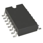 2309-1HDCG8
The activity of extra discounts on wholesale prices is in full swing…
Please fill in your contact information and we will send you the latest wholesale price list.





