 ChipApex | Global Electronic Components Supplier
SEARCH
Search Product
Search Post
— IC芯片 | 连接器 | 传感器 | 被动器件 —
Search productSearch post
— IC芯片 | 连接器 | 传感器 | 被动器件 —
Consult the customer manager about the wholesale price.
consultation hotline:86-132-6715-2157
email:[email protected]
Contact the product manager for consultation. One-stop consultation is available.
Do you want a lower wholesale price? Please send us your inquiry and we will reply immediately.
The Renesas 2309A-1DCG is a 3.3V zero-delay low-skew clock buffer featuring a 16-pin SOIC package with a 1.27mm pitch. It distributes one reference input to nine outputs across two banks (four and five) using an on-chip PLL for phase alignment. The device operates at frequencies from 10MHz to 133MHz with output skew under 250ps and cycle-to-cycle jitter below 200ps. It supports tri-state mode, accepts LVTTL/LVCMOS inputs, and functions within the industrial temperature range of -40°C to 85°C.
Verify the specific suffix 'DCG' corresponds to the 16-pin SOIC package and industrial temperature grade (-40°C to 85°C). Confirm RoHS compliance status and moisture sensitivity level (MSL 3) requirements against current manufacturing notices. Ensure the ordering part number matches the exact drive strength variant required for the application.
Select the 2309A-1DCG for applications requiring precise phase alignment between input and output clocks without external components. Choose this over the standard 2309-1 if industrial temperature performance is mandatory. Verify that the 12mA drive capability meets the load requirements of the connected circuitry.
The 2309A series represents a high-speed PLL-based clock buffer family designed for low-jitter distribution. The 2309A-1DCG is the industrial-grade version packaged in SOIC, distinct from the commercial grade and TSSOP variants. It serves as a 16-pin expansion of the 5-output 2305A architecture.
Publicly confirmed substitute part numbers are not available in the provided documentation.
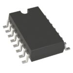 2309A-1DCG
The activity of extra discounts on wholesale prices is in full swing…
Please fill in your contact information and we will send you the latest wholesale price list.






