 ChipApex | Global Electronic Components Supplier
SEARCH
Search Product
Search Post
— IC芯片 | 连接器 | 传感器 | 被动器件 —
Search productSearch post
— IC芯片 | 连接器 | 传感器 | 被动器件 —
Consult the customer manager about the wholesale price.
consultation hotline:86-132-6715-2157
email:[email protected]
Contact the product manager for consultation. One-stop consultation is available.
Do you want a lower wholesale price? Please send us your inquiry and we will reply immediately.
The Renesas 2309A-1DCG8 is a high-speed, low-phase noise zero-delay clock buffer featuring an integrated Phase-Locked Loop (PLL). It accepts a single reference input and distributes the clock signal to two banks of outputs: one bank of four and another of five, totaling nine outputs. The device operates at frequencies up to 133 MHz with a supply voltage range of 3V to 3.6V. It utilizes LVTTL inputs and provides CMOS/LVCMOS/TTL outputs. Packaged in a 16-pin SOIC (0.154" width), it ensures low skew distribution for high-speed applications.
Verify the specific suffix 'DCG8' corresponds to the 16-pin SOIC package configuration. Confirm that the '1' designation indicates standard drive strength rather than the high-drive '-1H' variant. Ensure compatibility with the required operating temperature range, as commercial variants typically specify 0°C to 70°C while industrial versions extend to -40°C to 85°C.
Select this component when a zero-delay buffer is required to fan out a single clock source to nine destinations without external feedback networks. The 2309A-1DCG8 is suitable for designs needing separate enable controls for output banks. Verify that the 3.3V supply voltage and LVTTL input logic levels match the system requirements before integration.
This part belongs to the IDT/Renesas 2309 family of zero-delay buffers. The '2309A' denotes the specific generation with enhanced specifications compared to earlier revisions. The '1' suffix identifies the standard drive version, distinct from the '-1H' high-drive variant which offers faster rise and fall times. The 'DCG8' code specifies the 16-lead Small Outline Integrated Circuit package.
The 2309-1HDCGI8 is a related variant offering high drive strength and industrial temperature ratings (-40°C to 85°C) compared to the commercial range of the 2309A-1DCG8. Direct substitution requires verifying if the higher drive capability or extended temperature range is necessary for the specific application environment.
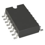 2309A-1DCG8
The activity of extra discounts on wholesale prices is in full swing…
Please fill in your contact information and we will send you the latest wholesale price list.





