 ChipApex | Global Electronic Components Supplier
SEARCH
Search Product
Search Post
— IC芯片 | 连接器 | 传感器 | 被动器件 —
Search productSearch post
— IC芯片 | 连接器 | 传感器 | 被动器件 —
Consult the customer manager about the wholesale price.
consultation hotline:86-132-6715-2157
email:[email protected]
Contact the product manager for consultation. One-stop consultation is available.
Do you want a lower wholesale price? Please send us your inquiry and we will reply immediately.
The Renesas Electronics Corporation IDT2309A-1HDCGI8 is a high-speed, 3.3V zero delay clock buffer featuring an on-chip phase-lock loop (PLL). It accepts one reference input and distributes the clock to two banks of four low-skew outputs (CLKA1–4 and CLKB1–4), plus an internal feedback CLKOUT pin. The -1H suffix indicates a high-drive version with faster rise and fall times compared to the standard drive variant. Operating frequencies range from 10 MHz to 133 MHz. The device supports separate output enables for each bank via S1 and S2 select inputs, allowing tri-state control or PLL bypass modes. It is characterized for industrial temperature operation (-40°C to +85°C) and housed in a 16-pin SOIC package.
Verify the ordering code matches the specific package and temperature grade required. The 'I' suffix denotes Industrial temperature range (-40°C to +85°C), while 'G' typically indicates lead-free/RoHS compliance. Confirm the 'H' suffix is present if high drive strength and faster slew rates are necessary for the design. Ensure the package type corresponds to the PCB footprint, as this part number specifies the SOIC package.
Select the IDT2309A-1HDCGI8 when high drive current and faster edge rates are required for heavy loads or long traces. The standard IDT2309A-1DCGI8 offers lower drive (8mA) which may suffice for lighter loads. Both variants share identical electrical characteristics regarding skew, jitter, and frequency range. Ensure all outputs, including unused ones, are loaded equally to maintain zero I/O delay performance.
The IDT2309A is a 16-pin derivative of the IDT2305A, expanding the output capacity from five to nine driven outputs (two banks of four). It belongs to the IDT2309 family of zero delay buffers. The manufacturer Integrated Device Technology (IDT) was acquired by Renesas Electronics Corporation, which now markets these components under the Renesas brand.
Publicly confirmed substitute part numbers are not available in the provided source material. Designers should consult official Renesas documentation for cross-reference information or verify compatibility with similar zero-delay buffers from other manufacturers based on pinout and electrical specifications.
Zero delay is achieved by aligning the phase between the incoming REF clock and the output clocks. This is done using an on-chip PLL where the feedback is obtained from the CLKOUT pad. All outputs, including CLKOUT, must be equally loaded to ensure true zero I/O delay.
The primary difference is the drive strength and switching speed. The -1H version is a high-drive device with a maximum rise/fall time of 1.5 ns and can sink/source up to 12 mA. The standard -1 version has a maximum rise/fall time of 2.5 ns and a drive capability of 8 mA.
Yes, the device allows separate output enable control for each bank. Setting S1 and S2 inputs to specific logic levels can place Bank A, Bank B, or both into tri-state mode, or bypass the PLL to drive outputs directly from the REF input.
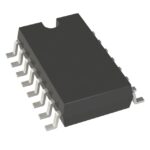 2309A-1HDCGI8
The activity of extra discounts on wholesale prices is in full swing…
Please fill in your contact information and we will send you the latest wholesale price list.






