 ChipApex | Global Electronic Components Supplier
SEARCH
Search Product
Search Post
— IC芯片 | 连接器 | 传感器 | 被动器件 —
Search productSearch post
— IC芯片 | 连接器 | 传感器 | 被动器件 —
Consult the customer manager about the wholesale price.
consultation hotline:86-132-6715-2157
email:[email protected]
Contact the product manager for consultation. One-stop consultation is available.
Do you want a lower wholesale price? Please send us your inquiry and we will reply immediately.
The 23S08-1DCGI is a 3.3V Zero Delay Clock Multiplier manufactured by Renesas Electronics, designed for high-speed clock distribution and multiplication applications. It operates within an input frequency range of 10 MHz to 133 MHz using LVCMOS input signals. The device features one input and eight outputs distributed across two banks, with an output frequency range of 10 MHz to 133 MHz. Key electrical parameters include a maximum cycle-to-cycle jitter of 200 ps and an output skew of 200 ps. It accepts spread spectrum inputs and functions at a core voltage of 3.3 V. The component is housed in a 16-lead SOIC package (DCG) with dimensions of 9.9 x 3.9 x 1.5 mm and a pitch of 1.27 mm.
Verify the obsolete status of this part number before procurement planning. Confirm that the SOIC-16 package dimensions and pinout match the target PCB footprint. Ensure the 3.3V supply voltage and LVCMOS signal levels are compatible with the system design requirements.
Select the 23S08-1DCGI when a single input clock needs to be buffered and multiplied by a factor of one to eight outputs with zero delay. This model is suitable for commercial temperature ranges (0 to 70°C). Consider alternative suffixes if industrial temperature ratings or different package types like TSSOP are required.
This component belongs to the 23S08 family of zero delay buffers. It shares functional characteristics with variants such as the 23S08-2HDCG, which supports 1x and 2x multiplication, and the 23S08-1HPGG, which utilizes a TSSOP package. The specific -1DCGI suffix indicates the 1x multiplier configuration in the standard SOIC package.
Direct substitutes within the same package include other 23S08 variants like the 23S08-1DCG. For package changes, the 23S08-1HPGG offers the same 1x functionality in a TSSOP-16 form factor. Verify pin compatibility when switching between SOIC and TSSOP packages.
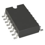 23S08-1DCGI
The activity of extra discounts on wholesale prices is in full swing…
Please fill in your contact information and we will send you the latest wholesale price list.






