 ChipApex | Global Electronic Components Supplier
SEARCH
Search Product
Search Post
— IC芯片 | 连接器 | 传感器 | 被动器件 —
Search productSearch post
— IC芯片 | 连接器 | 传感器 | 被动器件 —
Consult the customer manager about the wholesale price.
consultation hotline:86-132-6715-2157
email:[email protected]
Contact the product manager for consultation. One-stop consultation is available.
Do you want a lower wholesale price? Please send us your inquiry and we will reply immediately.
The Renesas 23S08-1HDCG8 is a 3.3V zero-delay clock multiplier with spread spectrum compatibility, housed in a 16-pin SOIC package. It accepts LVCMOS input frequencies from 10 MHz to 133 MHz and provides eight LVCMOS outputs. The device features a maximum cycle-to-cycle jitter of 200 ps and output skew of 200 ps. Operating within a commercial temperature range of 0°C to +70°C, it utilizes an external feedback pin for phase synchronization. The component supports 1x multiplication/division and includes power-down capabilities.
Verify the specific suffix '8' against official documentation to confirm tape-and-reel packaging versus tube variants. Confirm RoHS compliance status and moisture sensitivity level (MSL 3) prior to assembly planning. Ensure the selected variant matches the required 1x multiplication factor and LVCMOS output specifications.
Select this component when a single LVCMOS source must drive multiple loads with minimal phase delay. The 23S08-1HDCG8 is suitable for designs operating between 10 MHz and 133 MHz. Consider the 16-pin SOIC footprint for PCB layout constraints. Verify that the application does not require differential outputs or higher frequency ranges exceeding 133 MHz.
This part belongs to the IDT/Renesas 23S08 family of zero-delay buffers. It serves as a high-speed clock multiplier designed to replace crystal oscillators in complex digital systems. The device aligns output edges with the input reference to eliminate propagation delay errors common in standard buffer circuits.
The 23S08-1HDCG is a comparable tube-packaged variant within the same series. Cross-reference pinouts and electrical parameters carefully when substituting.
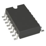 23S08-1HDCG8
The activity of extra discounts on wholesale prices is in full swing…
Please fill in your contact information and we will send you the latest wholesale price list.





