 ChipApex | Global Electronic Components Supplier
SEARCH
Search Product
Search Post
— IC芯片 | 连接器 | 传感器 | 被动器件 —
Search productSearch post
— IC芯片 | 连接器 | 传感器 | 被动器件 —
Consult the customer manager about the wholesale price.
consultation hotline:86-132-6715-2157
email:[email protected]
Contact the product manager for consultation. One-stop consultation is available.
Do you want a lower wholesale price? Please send us your inquiry and we will reply immediately.
The Renesas Electronics 23S08-2DCG8 is a 3.3V zero-delay clock multiplier designed for high-speed digital systems. It features eight LVCMOS outputs and supports input frequencies ranging from 10 MHz to 133 MHz, with an output frequency range of 10 MHz to 133 MHz. The device operates within a commercial temperature range of 0°C to +70°C and consumes 45 mA of supply current. Key performance metrics include a maximum center-to-center jitter of 200 ps and an output skew of 200 ps. It is housed in a 16-pin SOIC package.
This component is identified as obsolete or end-of-life (EOL) by major distributors. Verification of availability requires checking secondary market suppliers or authorized stockists for remaining inventory. Buyers must confirm the specific suffix '8' indicates tape-and-reel packaging if required for automated assembly processes.
Select this part when a zero-delay clock multiplication function is needed with up to eight outputs at frequencies up to 133 MHz. Ensure the design accommodates the 200 ps jitter specification. Verify that the SOIC-16 package footprint matches the PCB layout constraints and that the 3.3V logic levels are compatible with the receiving devices.
The 23S08 series belongs to Renesas' family of zero-delay clock multipliers, originally developed by Integrated Device Technology (IDT). These components are widely used in legacy designs requiring low-skew clock distribution. The 23S08-2DCG8 variant specifically denotes the 3.3V operation, SOIC package, and reel packaging configuration.
Direct pin-compatible replacements may be found within the same 23S08 family, such as the 23S08-2DCG (tube packaging) or 23S08-1HPGG (TSSOP package), provided the package type change is acceptable. Cross-reference with newer Femtoclock series devices for improved jitter performance if system requirements allow.
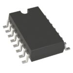 23S08-2DCG8
The activity of extra discounts on wholesale prices is in full swing…
Please fill in your contact information and we will send you the latest wholesale price list.





