 ChipApex | Global Electronic Components Supplier
SEARCH
Search Product
Search Post
— IC芯片 | 连接器 | 传感器 | 被动器件 —
Search productSearch post
— IC芯片 | 连接器 | 传感器 | 被动器件 —
Consult the customer manager about the wholesale price.
consultation hotline:86-132-6715-2157
email:[email protected]
Contact the product manager for consultation. One-stop consultation is available.
Do you want a lower wholesale price? Please send us your inquiry and we will reply immediately.
The Renesas Electronics 23S09-1DCGI is a high-speed phase-locked loop (PLL) clock buffer designed for zero-delay clock distribution. It accepts one reference input and drives two banks of four low-skew outputs, totaling nine outputs. The device operates within a frequency range of 10MHz to 133MHz at 3.3V. It features an on-chip PLL that locks to the input clock on the REF pin, with feedback obtained from the CLKOUT pad. In the absence of an input clock, the device enters a power-down mode with less than 12μA current draw in the commercial temperature range.
Verify the specific suffix 'I' for industrial temperature range (-40°C to +85°C) against the required operating conditions. Confirm package type is 16-SOIC. Check RoHS compliance status as it varies by manufacturing date. Ensure compatibility with LVTTL input levels. Consult official datasheets for moisture sensitivity level handling requirements before assembly.
Select this component when a single clock source needs to be distributed to multiple loads with minimal skew. The -1H variant offers higher drive strength if load capacitance exceeds standard specifications. Ensure the application frequency falls within the 10MHz to 133MHz operational range. Verify that the 3.3V supply voltage matches the system design constraints.
This part belongs to the 23S09 family of zero-delay buffers. It is a 16-pin version derived from the 23S05 series. The device is manufactured by Renesas Electronics Corporation, formerly IDT. It is available in SOIC packages. The -1 designation indicates standard drive capability compared to the -1H high-drive version.
Public confirmed substitute part numbers are not provided in the verified source material. Evaluate alternative clock buffers based on pin compatibility, electrical specifications, and package dimensions. Verify functional equivalence regarding PLL configuration and output drive strength before substitution.
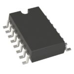 23S09-1DCGI
The activity of extra discounts on wholesale prices is in full swing…
Please fill in your contact information and we will send you the latest wholesale price list.






