 ChipApex | Global Electronic Components Supplier
SEARCH
Search Product
Search Post
— IC芯片 | 连接器 | 传感器 | 被动器件 —
Search productSearch post
— IC芯片 | 连接器 | 传感器 | 被动器件 —
Consult the customer manager about the wholesale price.
consultation hotline:86-132-6715-2157
email:[email protected]
Contact the product manager for consultation. One-stop consultation is available.
Do you want a lower wholesale price? Please send us your inquiry and we will reply immediately.
The Renesas 2510CGLF is a 3.3V phase-lock loop clock driver designed for synchronous SDRAM applications. It aligns the CLKOUT signal with the CLKIN signal in both phase and frequency using PLL technology. The device distributes one clock input to ten outputs, meeting PC133 registered DIMM specifications. It operates at frequencies between 25MHz and 175MHz and supports spread spectrum clocking. The component is housed in a plastic 24-pin TSSOP package (173mil) and functions within a commercial temperature range of 0°C to 70°C.
Verify the specific suffix 'GLF' against current manufacturer documentation to confirm lead-free status and RoHS compliance. Confirm the active status as datasheets may list variants like 2510CG as obsolete while others remain available. Ensure the package type matches the required 24-TSSOP footprint for PCB integration.
Select this component when a low-skew, low-jitter clock distribution solution is required for synchronous memory interfaces. The 1:10 fan-out ratio suits designs needing multiple synchronized clock lines from a single source. Verify that the 3.3V supply voltage aligns with the system power architecture and that the 0°C to 70°C operating range meets environmental requirements.
The 2510CGLF belongs to the 2510C family of VersaClock devices. This series focuses on high-performance clock generation and distribution for memory subsystems. The 'GLF' suffix typically denotes a lead-free and RoHS-compliant variant of the standard 2510C part, packaged in a 24-pin TSSOP.
Check for direct pin-compatible replacements within the same VersaClock family or newer generations such as the 5P series if the 2510CGLF is discontinued. Verify electrical parameters including voltage levels and output drive strength before substituting.
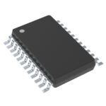 2510CGLF
The activity of extra discounts on wholesale prices is in full swing…
Please fill in your contact information and we will send you the latest wholesale price list.





