 ChipApex | Global Electronic Components Supplier
SEARCH
Search Product
Search Post
— IC芯片 | 连接器 | 传感器 | 被动器件 —
Search productSearch post
— IC芯片 | 连接器 | 传感器 | 被动器件 —
Consult the customer manager about the wholesale price.
consultation hotline:86-132-6715-2157
email:[email protected]
Contact the product manager for consultation. One-stop consultation is available.
Do you want a lower wholesale price? Please send us your inquiry and we will reply immediately.
The onsemi 2N7002W is a small signal N-channel enhancement mode MOSFET housed in an SC-70 (SOT-323) surface-mount package. It features a drain-to-source voltage rating of 60 V and a maximum continuous drain current of 340 mA at 25°C. The device exhibits a low on-resistance of 1.6 Ω at VGS = 10 V and 2.5 Ω at VGS = 4.5 V. Total gate charge is typically 0.7 nC, supporting efficient switching. Operating junction temperature ranges from -55°C to +150°C with a steady-state power dissipation of 280 mW.
Verify the specific ordering suffix to confirm packaging format and automotive qualification status. Confirm that the selected variant meets AEC-Q101 requirements if the application demands unique site or control change protocols. Ensure compliance with RoHS and halogen-free standards during procurement.
Select this component for space-constrained designs requiring a compact SC-70 footprint. Consider the 60 V breakdown voltage and 340 mA current capability for general-purpose switching tasks. Evaluate thermal performance based on the specified junction-to-ambient resistance values under your specific board layout conditions.
This part belongs to the 2N7002W series of single N-channel MOSFETs manufactured by onsemi. It is designed for small-signal applications where low on-resistance and high ESD protection are critical. The device is available in lead-free, halogen-free, and BFR-free configurations.
The 2V7002WT1G is a confirmed substitute within the same family, offering identical electrical characteristics while meeting additional automotive qualification requirements including PPAP capability.
The typical total gate charge (QG(TOT)) is 0.7 nC when tested at VGS = 4.5 V, VDS = 10 V, and ID = 200 mA.
Yes, the 2V7002W variant is AEC-Q101 qualified and PPAP capable, making it suitable for automotive and other applications requiring unique site and control change requirements.
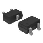 2N7002W
The activity of extra discounts on wholesale prices is in full swing…
Please fill in your contact information and we will send you the latest wholesale price list.





