 ChipApex | Global Electronic Components Supplier

SEARCH
Search Product
Search Post
— IC芯片 | 连接器 | 传感器 | 被动器件 —
Search productSearch post
— IC芯片 | 连接器 | 传感器 | 被动器件 —
Consult the customer manager about the wholesale price.
consultation hotline:86-132-6715-2157
email:[email protected]
Contact the product manager for consultation. One-stop consultation is available.
Do you want a lower wholesale price? Please send us your inquiry and we will reply immediately.
2SC5172(YAZK,Q,M) is listed in the Single Bipolar Transistors range at ChipApex. The manufacturer field lists Toshiba Semiconductor and Storage. Its product description is TRANS NPN 400V 5A TO-220NIS. Review the specifications below when checking this part for your BOM.
The Toshiba 2SC5172 is a silicon NPN triple-diffused transistor utilizing the PCT process. It features a collector-emitter breakdown voltage of 400 V and a DC collector current rating of 5 A. The device exhibits excellent switching performance with a maximum rise time of 0.5 μs and fall time of 0.3 μs at 2 A. Electrical characteristics include a minimum DC current gain of 20 at 0.5 A, a collector cut-off current of 20 μA, and a collector-base breakdown voltage of 600 V. It operates within a junction temperature range up to 150 °C.
Verify component authenticity through authorized distributors or direct manufacturer channels. Confirm RoHS compliance status by contacting sales representatives as specified in the documentation. Ensure designs adhere to absolute maximum ratings and derating guidelines found in the Toshiba Semiconductor Reliability Handbook to maintain operational safety and longevity.
Select this component for designs requiring high-voltage handling and rapid switching transitions. Evaluate thermal management requirements against the 2 W dissipation limit at ambient conditions versus 25 W at case temperature. Verify that load currents remain within the safe operating area curves provided in the datasheet to prevent device failure during transient events.
This device belongs to the family of high-voltage NPN transistors designed for power conversion tasks. It utilizes a TO-220 package variant suitable for through-hole mounting. The part number suffixes indicate specific ordering or packaging variations without altering the fundamental electrical specifications defined in the primary datasheet.
Public confirmed substitute part numbers are not available in the verified source material.
The maximum collector-emitter saturation voltage is 1.0 V when tested at a collector current of 2 A and a base current of 0.25 A.
The minimum DC current gain is 13 at 1 mA and increases to a minimum of 20 at 0.5 A, with a maximum rated gain of 65 under the same 0.5 A condition.
The storage time is typically 2.0 μs under test conditions involving a base drive of 0.25 A and a reverse base drive of -0.5 A with a duty cycle less than 1%.
Explore related parts through Bipolar (BJT), Transistors, Discrete Semiconductor Products, all product categories.
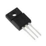 2SC5172(YAZK,Q,M)

The activity of extra discounts on wholesale prices is in full swing…
Please fill in your contact information and we will send you the latest wholesale price list.





