 ChipApex | Global Electronic Components Supplier
SEARCH
Search Product
Search Post
— IC芯片 | 连接器 | 传感器 | 被动器件 —
Search productSearch post
— IC芯片 | 连接器 | 传感器 | 被动器件 —
Consult the customer manager about the wholesale price.
consultation hotline:86-132-6715-2157
email:[email protected]
Contact the product manager for consultation. One-stop consultation is available.
Do you want a lower wholesale price? Please send us your inquiry and we will reply immediately.
The Toshiba 2SJ610 is a silicon P-channel MOSFET utilizing π-MOSV technology, designed for switching regulator, DC/DC converter, and motor drive applications. It features a drain-source voltage rating of -250 V and a continuous drain current of -2.0 A. The device exhibits a typical drain-source ON-resistance of 1.85 Ω and a forward transfer admittance of 1.8 S. Key electrical characteristics include a gate threshold voltage ranging from -1.5 to -3.5 V and a maximum gate-source voltage of ±20 V. Thermal performance includes a channel-to-case thermal resistance of 6.25 °C/W and a maximum channel temperature of 150 °C.
Verify the specific ordering suffix against official Toshiba documentation to confirm package type and environmental compliance status. Confirm availability as distribution channels may vary. Ensure design accounts for absolute maximum ratings, particularly regarding avalanche energy limits and thermal derating curves under heavy loads.
Select this component for designs requiring high-voltage P-channel switching capabilities up to 250 V. Evaluate the thermal resistance and safe operating area (SOA) to ensure the junction temperature remains within limits during pulsed operations. Consider the gate charge requirements for driver circuit compatibility in high-frequency switching environments.
This device belongs to Toshiba's discrete field-effect transistor portfolio, specifically engineered for general electronics and industrial applications. It serves as a high-voltage switching element suitable for replacing older bipolar or standard MOS technologies where lower on-resistance and faster switching speeds are required in compact surface-mount packages.
Consult official Toshiba substitution guides for verified equivalents. Cross-reference pinouts, thermal resistance values, and breakdown voltages carefully when considering alternative manufacturers' parts to ensure functional compatibility without redesigning the PCB layout.
The maximum single-pulse avalanche energy (EAS) is rated at 180 mJ under test conditions of VDD = -50 V, initial Tch = 25°C, L = 75 mH, IAR = -2.0 A, and RG = 25 Ω.
Yes, the device supports repetitive avalanche energy (EAR) rated at 2.0 mJ, provided the pulse width is limited by the maximum channel temperature constraints.
The reverse recovery time (trr) is typically 120 ns when tested with IDR = -2.0 A, VGS = 0 V, and dIDR/dt = 100 A/μs.
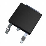 2SJ610(TE16L1,NQ)
The activity of extra discounts on wholesale prices is in full swing…
Please fill in your contact information and we will send you the latest wholesale price list.





