ChipApex | Global Electronic Components Supplier
SEARCH
Search Product
Search Post
— IC芯片 | 连接器 | 传感器 | 被动器件 —
Search productSearch post
— IC芯片 | 连接器 | 传感器 | 被动器件 —
Consult the customer manager about the wholesale price.
consultation hotline:86-132-6715-2157
email:[email protected]
Contact the product manager for consultation. One-stop consultation is available.
Do you want a lower wholesale price? Please send us your inquiry and we will reply immediately.
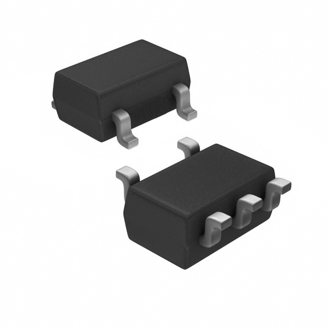
The Toshiba 2SK2145-Y(TE85L,F) is a dual N-channel junction field-effect transistor (JFET) housed in an SM5 surface-mount package. It features a gate-drain breakdown voltage of -50 V and a total drain power dissipation of 300 mW. The Y suffix designates a specific drain current classification with a minimum of 1.2 mA and a maximum of 3.0 mA at VDS = 10 V and VGS = 0. The device provides a typical forward transfer admittance of 15 mS and achieves a noise figure of 1.0 dB under standard test conditions.
Verify the ordering suffix matches the required drain current specification, as the Y designation indicates a specific Idss range of 1.2 to 3.0 mA. Confirm the package type is SM5 and ensure compliance with RoHS standards. Review the Toshiba Semiconductor Reliability Handbook for derating guidelines before finalizing procurement specifications.
Select this component when a dual JFET configuration is required within a small footprint. The Y variant is appropriate for designs needing lower drain current compared to GR or BL classifications. Ensure the application operates within the specified junction temperature limits and accounts for the total power dissipation rating across both internal devices.
This part belongs to the 2SK2145 series of silicon N-channel junction FETs designed specifically for audio frequency low noise amplifier applications. The series utilizes a common-source configuration with two elements per package. The TE85L,F suffix denotes the specific tape-and-reel packaging format used for automated surface-mount assembly processes.
Direct substitutes include other 2SK2145 variants such as the 2SK2145-GR and 2SK2145-BL, which share identical electrical characteristics but differ in drain current classification ranges. Verify that the alternative variant's Idss limits align with the circuit requirements.
 2SK2145-Y(TE85L,F)
The activity of extra discounts on wholesale prices is in full swing…
Please fill in your contact information and we will send you the latest wholesale price list.