 ChipApex | Global Electronic Components Supplier
SEARCH
Search Product
Search Post
— IC芯片 | 连接器 | 传感器 | 被动器件 —
Search productSearch post
— IC芯片 | 连接器 | 传感器 | 被动器件 —
Consult the customer manager about the wholesale price.
consultation hotline:86-132-6715-2157
email:[email protected]
Contact the product manager for consultation. One-stop consultation is available.
Do you want a lower wholesale price? Please send us your inquiry and we will reply immediately.
The Toshiba 2SK3309(Q) is a silicon N-channel MOS field-effect transistor designed for switching regulator applications. It features a low drain-source ON resistance of 0.48 Ω (typical) and high forward transfer admittance of 4.3 S (typical). The device supports a maximum drain-source voltage of 450 V and a continuous DC drain current of 10 A, with pulse currents reaching 40 A. Key electrical characteristics include a gate threshold voltage between 3.0 V and 5.0 V, a maximum gate leakage current of ±10 μA, and a maximum drain cut-off current of 100 μA at 450 V. Thermal performance includes a channel-to-case thermal resistance of 1.92 °C/W.
Verify the specific ordering suffix against official Toshiba Semiconductor documentation to confirm package type and marking details. Ensure compliance with export regulations and intended use restrictions outlined in the datasheet. Confirm environmental compliance status directly with the manufacturer or authorized distributor as RoHS compatibility requires specific verification.
Select this component for designs requiring high-voltage N-channel switching with moderate current capabilities. Evaluate the thermal resistance and safe operating area curves to ensure adequate heat dissipation under expected load conditions. Consider the gate charge parameters when designing drive circuits to optimize switching speed and minimize losses.
This part belongs to Toshiba's silicon N-channel MOSFET lineup utilizing π-MOSV technology. It is engineered specifically for power conversion efficiency in general-purpose electronic equipment. The device represents a balance between conduction losses and switching performance suitable for standard frequency switching regulators.
Consult official Toshiba cross-reference lists for verified substitutes. Ensure any replacement matches the 450 V rating, 10 A current capacity, and compatible pinout configuration without altering the circuit design requirements.
The typical forward transfer admittance (|Yfs|) is 4.3 S when measured at VDS = 10 V and ID = 5 A.
Yes, the device is rated for single-pulse avalanche energy of 222 mJ and repetitive avalanche energy of 6.5 mJ under specified test conditions.
The minimum drain-source breakdown voltage (V(BR)DSS) is 450 V when tested at ID = 10 mA and VGS = 0 V.
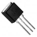 2SK3309(Q)
The activity of extra discounts on wholesale prices is in full swing…
Please fill in your contact information and we will send you the latest wholesale price list.





