ChipApex | Global Electronic Components Supplier
SEARCH
Search Product
Search Post
— IC芯片 | 连接器 | 传感器 | 被动器件 —
Search productSearch post
— IC芯片 | 连接器 | 传感器 | 被动器件 —
Consult the customer manager about the wholesale price.
consultation hotline:86-132-6715-2157
email:[email protected]
Contact the product manager for consultation. One-stop consultation is available.
Do you want a lower wholesale price? Please send us your inquiry and we will reply immediately.
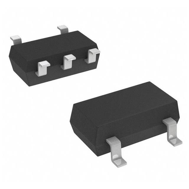
The Toshiba 2SK3320-BL(TE85L,F) is a silicon N-channel junction field-effect transistor (JFET) designed for low noise audio amplifier applications. It features an ultra super mini five-pin package containing two devices. The BL suffix indicates a drain current classification of 6.0 to 14.0 mA. Key electrical characteristics include a high forward transfer admittance of 15 mS typical, a gate-drain breakdown voltage of -50 V, and a super low noise figure of 1.0 dB at 1 kHz. The device offers high input impedance with a maximum gate-source cut-off current of -1 nA.
Verify the specific ordering suffix matches the required drain current classification, as the BL designation corresponds to a defined IDSS range. Confirm the package type and pin assignment align with the design schematic. Ensure compliance with environmental directives such as RoHS before finalizing procurement specifications.
Select this component when designing circuits requiring minimal noise contribution from the initial amplification stage. The dual configuration allows for balanced differential inputs within a compact footprint. Consider the absolute maximum ratings for thermal management and ensure the operating conditions remain within the specified junction temperature limits.
This part belongs to Toshiba's lineup of silicon N-channel junction field-effect transistors specifically engineered for analog signal processing. The 2SK3320 series provides matched pairs in a single package to facilitate precise circuit balancing. It serves as a specialized alternative to discrete JFETs where size constraints and noise performance are critical design factors.
Direct replacements must match the five-pin package outline and electrical parameters. Verify that substitute components offer comparable noise figures and forward transfer admittance to maintain circuit performance integrity.
The 'BL' suffix specifies the Drain Current (IDSS) classification, which ranges from 6.0 to 14.0 mA under standard test conditions.
The package contains two independent JFET devices configured in a single ultra super mini five-pin housing.
The typical noise figure is 1.0 dB when measured at VDS = 10 V, RG = 1 kΩ, ID = 0.5 mA, and f = 1 kHz.
 2SK3320-BL(TE85L,F
The activity of extra discounts on wholesale prices is in full swing…
Please fill in your contact information and we will send you the latest wholesale price list.