 ChipApex | Global Electronic Components Supplier
SEARCH
Search Product
Search Post
— IC芯片 | 连接器 | 传感器 | 被动器件 —
Search productSearch post
— IC芯片 | 连接器 | 传感器 | 被动器件 —
Consult the customer manager about the wholesale price.
consultation hotline:86-132-6715-2157
email:[email protected]
Contact the product manager for consultation. One-stop consultation is available.
Do you want a lower wholesale price? Please send us your inquiry and we will reply immediately.
The Toshiba Semiconductor and Storage 2SK3342 is a silicon N-channel MOSFET utilizing π-MOSV technology, designed for switching regulators, DC-DC converters, and motor drives. It features a drain-source voltage of 250 V and a continuous drain current of 4.5 A at 25°C case temperature. The device exhibits a typical drain-source ON resistance of 0.8 Ω and a forward transfer admittance of 4.5 S. Gate threshold voltage ranges from 1.5 to 3.5 V. It operates with a maximum channel temperature of 150°C and supports repetitive avalanche energy of 2.0 mJ.
Verify the specific ordering suffix against official Toshiba documentation to confirm environmental compliance status, such as RoHS compatibility. Confirm package dimensions and marking details match the required JEDEC or Toshiba standards. Ensure thermal management design accounts for the specified thermal resistance values to maintain safe operating temperatures under load conditions.
Select this component when designing circuits requiring a 250 V N-channel MOSFET with moderate current handling capabilities. Consider the 0.8 Ω ON resistance for efficiency requirements and the 4.5 A continuous current rating for load matching. Evaluate the gate threshold voltage range to ensure compatibility with available logic level drivers or gate drive voltages.
This part belongs to the family of silicon N-channel MOSFETs manufactured by Toshiba Semiconductor and Storage. It is specifically engineered using π-MOSV technology to optimize switching characteristics and on-resistance. The device is intended for general electronics applications, including industrial and consumer equipment, where reliable power switching is required.
Consult official Toshiba documentation for confirmed substitute part numbers. Verify that any replacement matches the 250 V drain-source voltage, 4.5 A current rating, and compatible pinout configuration.
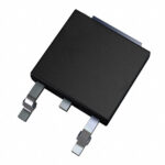 2SK3342(TE16L1,NQ)
The activity of extra discounts on wholesale prices is in full swing…
Please fill in your contact information and we will send you the latest wholesale price list.





