ChipApex | Global Electronic Components Supplier
SEARCH
Search Product
Search Post
— IC芯片 | 连接器 | 传感器 | 被动器件 —
Search productSearch post
— IC芯片 | 连接器 | 传感器 | 被动器件 —
Consult the customer manager about the wholesale price.
consultation hotline:86-132-6715-2157
email:[email protected]
Contact the product manager for consultation. One-stop consultation is available.
Do you want a lower wholesale price? Please send us your inquiry and we will reply immediately.
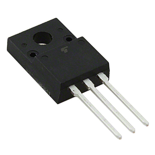
The Toshiba 2SK4016 is a silicon N-channel MOS field-effect transistor utilizing π-MOS VI technology, designed for switching regulator applications. It features a drain-source voltage rating of 600 V and a continuous DC drain current capacity of 13 A at a case temperature of 25°C. The device exhibits a typical drain-source ON-resistance of 0.33 Ω and a forward transfer admittance of 10 S. Key electrical characteristics include a gate threshold voltage range of 2.0 to 4.0 V and a maximum gate leakage current of ±10 μA. Thermal performance is defined by a channel-to-case thermal resistance of 2.5 °C/W.
Verify the specific ordering suffix and lot number markings on the component body to confirm environmental compliance status, such as RoHS compatibility, as indicated in the datasheet. Ensure that the procurement documentation aligns with the manufacturer's latest reliability handbook and handling precautions. Confirm the package type matches the JEDEC SC-67 or Toshiba 2-10U1B specifications before integration into designs.
Select this component for designs requiring a 600 V breakdown voltage and up to 13 A continuous current capability. Consider the thermal resistance of 2.5 °C/W when designing heat dissipation strategies for case temperatures. Evaluate the gate threshold voltage range of 2.0 to 4.0 V to ensure compatibility with the intended drive circuitry logic levels. Account for the single-pulse avalanche energy rating of 1033 mJ if transient overvoltage protection is required within the system architecture.
This device belongs to the Toshiba Field Effect Transistor series, specifically employing Silicon N-Channel MOS technology. It is categorized under discrete semiconductors intended for general electronic applications. The product line emphasizes reliability through adherence to specific manufacturing standards and includes detailed thermal and electrical characterization data for design validation purposes.
Publicly confirmed substitute part numbers are not available in the provided source material. Consult the manufacturer directly for potential alternatives or updated product lines.
The maximum channel temperature (Tch) is rated at 150 °C.
The gate-source breakdown voltage (V(BR)GSS) is specified as ±30 V with a gate current of ±10 μA.
The typical total gate charge (Qg) is 62 nC under test conditions of VDD ≈ 400 V, VGS = 10 V, and ID = 13 A.
 2SK4016(Q)
The activity of extra discounts on wholesale prices is in full swing…
Please fill in your contact information and we will send you the latest wholesale price list.