ChipApex | Global Electronic Components Supplier
SEARCH
Search Product
Search Post
— IC芯片 | 连接器 | 传感器 | 被动器件 —
Search productSearch post
— IC芯片 | 连接器 | 传感器 | 被动器件 —
Consult the customer manager about the wholesale price.
consultation hotline:86-132-6715-2157
email:[email protected]
Contact the product manager for consultation. One-stop consultation is available.
Do you want a lower wholesale price? Please send us your inquiry and we will reply immediately.
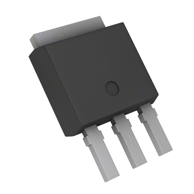
The Toshiba 2SK4021(Q) is a silicon N-channel MOSFET utilizing π-MOS V technology, designed for switching regulators and motor drives. It features a drain-source voltage of 250 V and a continuous DC drain current of 4.5 A at 25°C case temperature. The device exhibits a typical drain-source ON-resistance of 0.8 Ω and a forward transfer admittance of 4.5 S. It operates in enhancement mode with a gate threshold voltage between 1.5 V and 3.5 V. The component supports a pulse drain current of 18 A and dissipates up to 20 W at 25°C. It is housed in a TO-220AB package.
Verify the specific suffix (Q) against official Toshiba documentation to confirm environmental compliance status, such as RoHS compatibility, as standard markings may vary. Ensure the ordering information matches the exact pinout and thermal resistance specifications required for your heat sink design. Confirm that the requested quantity aligns with manufacturer distribution channels rather than third-party stock claims.
Select this component when a 250 V rating and 4.5 A continuous current are required in a TO-220AB package. Consider its 0.8 Ω ON-resistance for conduction loss calculations in power supply designs. Evaluate the 6.25 °C/W thermal resistance for heatsinking needs. Verify that the 1.5 V to 3.5 V threshold voltage is compatible with your logic or gate driver output levels.
This part belongs to the Toshiba Field Effect Transistor series employing Silicon N-Channel MOS Type technology. It is engineered specifically for general electronics applications where moderate power switching is needed. The device is distinct from higher-power industrial modules, focusing on compact TO-220AB integration for consumer and industrial equipment.
Consult Toshiba's official cross-reference guides for verified substitutes. Ensure any replacement maintains the 250 V D-S voltage, 4.5 A current rating, and TO-220AB footprint. Verify that the alternative device meets the same electrical life and thermal performance standards.
 2SK4021(Q)
The activity of extra discounts on wholesale prices is in full swing…
Please fill in your contact information and we will send you the latest wholesale price list.