 ChipApex | Global Electronic Components Supplier
SEARCH
Search Product
Search Post
— IC芯片 | 连接器 | 传感器 | 被动器件 —
Search productSearch post
— IC芯片 | 连接器 | 传感器 | 被动器件 —
Consult the customer manager about the wholesale price.
consultation hotline:86-132-6715-2157
email:[email protected]
Contact the product manager for consultation. One-stop consultation is available.
Do you want a lower wholesale price? Please send us your inquiry and we will reply immediately.
The Renesas 49FCT3805BSOG8 is a dual 1-to-5 clock driver and buffer built using advanced CMOS technology. It operates within a supply voltage range of 3V to 3.6V and supports input signals compatible with CMOS and LVTTL standards. The device features two independent driver banks, each providing a 1:5 fanout ratio with dedicated output enable controls. Designed for high-speed clock distribution, it ensures low skew and high signal quality. The component is housed in a 20-SOIC package and functions within an operating temperature range of -40°C to +85°C.
Verify the specific suffix 'SOG8' against official Renesas documentation to confirm pinout and electrical characteristics, as variations exist within the 49FCT3805 family. Confirm RoHS compliance status and check for End-of-Life notifications or Product Change Notices prior to procurement, as this component series has undergone discontinuance actions.
Select the 49FCT3805BSOG8 when dual independent clock domains with 1:5 fanout are required. Ensure the design utilizes 3.3V logic levels compatible with CMOS or LVTTL inputs. This part is suitable for designs needing on-chip diagnostics via the MON pin. Verify that the 20-SOIC package dimensions fit the PCB layout constraints.
This component belongs to the 49FCT3805 series of clock buffers and drivers. It shares functional similarities with variants such as the 49FCT3805ASOGI8 and 49FCT3805EPYGI, differing primarily in packaging and specific manufacturing lot codes. The 'B' suffix typically denotes a specific revision or binning within the Renesas IDT product lineage.
Official manufacturer-recommended replacements include the 5PB1106PGGI. Designers should verify that the substitute meets the specific 1:5 fanout and 3.3V operation requirements of the original design.
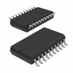 49FCT3805BSOG8
The activity of extra discounts on wholesale prices is in full swing…
Please fill in your contact information and we will send you the latest wholesale price list.





