ChipApex | Global Electronic Components Supplier
SEARCH
Search Product
Search Post
— IC芯片 | 连接器 | 传感器 | 被动器件 —
Search productSearch post
— IC芯片 | 连接器 | 传感器 | 被动器件 —
Consult the customer manager about the wholesale price.
consultation hotline:86-132-6715-2157
email:[email protected]
Contact the product manager for consultation. One-stop consultation is available.
Do you want a lower wholesale price? Please send us your inquiry and we will reply immediately.
The AD625 is a precision programmable gain instrumentation amplifier manufactured by Analog Devices Inc. The 5962-87719012A variant operates within an extended temperature range of -55°C to +125°C and utilizes a 20-terminal Leadless Chip Carrier package. It supports user-programmed gains from 1 to 10,000 via three external resistors. Key electrical specifications include a maximum gain error of 0.02%, a gain temperature coefficient of 5 ppm/°C, and a low input offset voltage of 25 µV. The device features a 25 MHz gain bandwidth product, 4 nV/√Hz input voltage noise at 1 kHz, and a 5 V/µs slew rate.
Verify the specific military drawing availability and ensure the 20-terminal LCC package matches the target footprint. Confirm that the extended temperature grade meets the operational requirements. Check for RoHS compliance status as manufacturing processes may vary. Validate pinout compatibility during integration to avoid circuit errors.
Select this component when fixed or programmable gains up to 10,000 are required with minimal external component count. Consider the 20-terminal LCC package for space-constrained designs. Evaluate the need for independent offset nulling if high precision is critical across varying temperatures. Ensure external resistor selection aligns with desired gain accuracy and temperature stability.
This part belongs to the AD625 family of precision instrumentation amplifiers designed for versatile gain control. It serves as a robust solution for applications demanding high CMRR and low drift. The military-grade variant ensures reliability in harsh environments. It complements other Analog Devices signal chain components for complete system integration.
Direct substitutes include other AD625 variants such as the AD625SE/883B for similar military specifications. Verify package dimensions and pinout compatibility before substitution. Ensure thermal performance meets the application's extended temperature requirements.
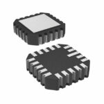 5962-87719012A
The activity of extra discounts on wholesale prices is in full swing…
Please fill in your contact information and we will send you the latest wholesale price list.