ChipApex | Global Electronic Components Supplier
SEARCH
Search Product
Search Post
— IC芯片 | 连接器 | 传感器 | 被动器件 —
Search productSearch post
— IC芯片 | 连接器 | 传感器 | 被动器件 —
Consult the customer manager about the wholesale price.
consultation hotline:86-132-6715-2157
email:[email protected]
Contact the product manager for consultation. One-stop consultation is available.
Do you want a lower wholesale price? Please send us your inquiry and we will reply immediately.
The AD841 is a wideband, unity-gain stable, fast settling operational amplifier fabricated using Analog Devices' junction isolated complementary bipolar process. It features a 40 MHz unity-gain bandwidth and a 300 V/µs slew rate. The device settles to within 0.01% of a 10 V step in 110 ns without long tails. DC performance includes a maximum input offset voltage of 1 mV for the K grade and a typical input voltage noise of 15 nV/√Hz. It provides a minimum output current drive of 50 mA with a maximum quiescent supply current of 12 mA.
Verify the specific suffix against the Ordering Guide to confirm package type and temperature range. The part number 5962-89641012A corresponds to the AD841SE/883B variant under standard military drawing specifications. Confirm that the required environmental rating matches the -55°C to +125°C range associated with this MIL-STD-883B designation before finalizing procurement.
Select this component when unity-gain stability and rapid settling are critical requirements. The AD841 offers a combination of precision and speed previously available only in hybrid circuits. Consider the K grade if minimizing input offset voltage is necessary to avoid external nulling. Ensure the application load does not exceed the capacitive driving limits without series isolation resistors to maintain stability.
The AD841 belongs to a family of wide bandwidth operational amplifiers from Analog Devices, including the AD842. While the AD842 requires a gain of two or greater for stability, the AD841 is fully stable at unity gain. Both utilize the same complementary bipolar process to deliver high precision and wideband AC performance in a monolithic configuration.
The AD841SE/883B is the specific military-grade version corresponding to the 5962-89641012A designation. Other variants include the AD841SQ for ceramic DIP packaging and the AD841SE for LCC packaging, all sharing the same electrical characteristics but differing in physical form factor and qualification standards.
No, the AD841 is internally compensated and remains stable over its full operating temperature range without external components.
The absolute maximum differential input voltage is ±6 V. Exceeding this limit may damage the device.
The AD841 can drive capacitive loads up to 20 pF without performance degradation. For larger loads, a series resistor should be used to decouple the feedback loop and prevent instability.
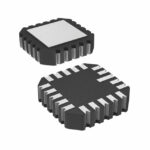 5962-89641012A
The activity of extra discounts on wholesale prices is in full swing…
Please fill in your contact information and we will send you the latest wholesale price list.