 ChipApex | Global Electronic Components Supplier
SEARCH
Search Product
Search Post
— IC芯片 | 连接器 | 传感器 | 被动器件 —
Search productSearch post
— IC芯片 | 连接器 | 传感器 | 被动器件 —
Consult the customer manager about the wholesale price.
consultation hotline:86-132-6715-2157
email:[email protected]
Contact the product manager for consultation. One-stop consultation is available.
Do you want a lower wholesale price? Please send us your inquiry and we will reply immediately.
The Altera 5AGXFB1H6F40C6N is an Arria V GX Field Programmable Gate Array (FPGA) designed for high-performance digital signal processing and connectivity applications. It features a dense logic architecture with 300,000 Logic Elements (LEs), organized into 11,320 Logic Array Blocks (LABs). The device integrates 14.75 Mbits of embedded memory and includes 24 high-speed transceivers capable of data rates up to 6.5536 Gb/s. Operating at a maximum frequency of 1.05 GHz, it utilizes a 1.1 V supply voltage and is housed in a 1517-pin FBGA package suitable for surface-mount technology.
Verify component authenticity through authorized channels due to potential availability constraints. Confirm RoHS compliance status and moisture sensitivity level prior to assembly. Review the latest Product Change Notification documents for any recent labeling or specification updates that may affect integration timelines.
Evaluate the trade-off between the 1517-pin package size and pin count requirements against available PCB real estate. Ensure thermal management solutions accommodate the power dissipation characteristics of the 1.1 V core voltage. Compare transceiver density needs against alternative Arria V variants if lower I/O counts suffice.
This component belongs to the Arria V GX family, which targets cost-sensitive high-performance applications compared to the Stratix series. It shares architectural similarities with other Arria V devices but offers specific transceiver configurations optimized for general-purpose high-speed serial links rather than specialized RF or PCIe interfaces found in other sub-families.
Publicly confirmed direct substitute part numbers are not available in the provided documentation. Consider evaluating other Arria V GX variants within the same package footprint if pin compatibility is required, subject to independent verification of electrical specifications.
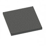 5AGXFB1H6F40C6N
The activity of extra discounts on wholesale prices is in full swing…
Please fill in your contact information and we will send you the latest wholesale price list.






