 ChipApex | Global Electronic Components Supplier
SEARCH
Search Product
Search Post
— IC芯片 | 连接器 | 传感器 | 被动器件 —
Search productSearch post
— IC芯片 | 连接器 | 传感器 | 被动器件 —
Consult the customer manager about the wholesale price.
consultation hotline:86-132-6715-2157
email:[email protected]
Contact the product manager for consultation. One-stop consultation is available.
Do you want a lower wholesale price? Please send us your inquiry and we will reply immediately.
The Renesas Electronics 5PB1104PGGI is a high-performance clock buffer within the 5PB1104 series, designed for mixed-signal applications. It features four LVCMOS outputs driven by an LVCMOS input, supporting maximum frequencies up to 200 MHz. The device operates on a supply voltage range of 1.71 V to 3.465 V and exhibits a maximum propagation delay of 2.4 ns. Packaged in an 8-lead TSSOP format, it functions reliably across an industrial temperature range from -40°C to +105°C with a typical operating current of 20 mA.
Verify component authenticity through authorized channels. Confirm RoHS compliance status via official documentation. Check for Product Change Notifications (PCN) regarding recent manufacturing updates. Ensure packaging specifications match design requirements, as tube quantities may vary.
Select this model when four buffered LVCMOS signals are required at frequencies up to 200 MHz. The TSSOP-8 package suits space-constrained designs. Verify that the 1.71 V to 3.465 V supply range aligns with system power rails. Consider the 20 mA operating current for thermal management calculations.
This component belongs to the 5PB1104 family of ultra-low jitter LVCMOS buffers manufactured by Renesas Electronics. The 'PGGI' suffix denotes specific packaging and environmental attributes within the product line. Related variants include the 5PB1104CMT1 and other members of the 5PB11xx series offering different output counts or package types.
The 5PB1104CMT1 serves as a functional alternative within the same series, offering identical electrical characteristics but differing in packaging configuration.
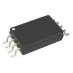 5PB1104PGGI
The activity of extra discounts on wholesale prices is in full swing…
Please fill in your contact information and we will send you the latest wholesale price list.






