 ChipApex | Global Electronic Components Supplier
SEARCH
Search Product
Search Post
— IC芯片 | 连接器 | 传感器 | 被动器件 —
Search productSearch post
— IC芯片 | 连接器 | 传感器 | 被动器件 —
Consult the customer manager about the wholesale price.
consultation hotline:86-132-6715-2157
email:[email protected]
Contact the product manager for consultation. One-stop consultation is available.
Do you want a lower wholesale price? Please send us your inquiry and we will reply immediately.
The Renesas Electronics 5PB1108CMGI8 is a high-performance LVCMOS clock buffer featuring a 1:8 fan-out configuration. It operates within a supply voltage range of 1.71 V to 3.465 V and supports maximum input frequencies up to 200 MHz. The device is housed in an 8-UFDFN package with dimensions of 2x2 mm. It functions reliably across an extended temperature range from -40°C to +105°C, ensuring stability in demanding industrial environments.
Verify the specific suffix 'CMGI8' against official Renesas documentation to confirm the package type (8-UFDFN) and temperature grade (+105°C). Ensure compatibility with existing PCB footprints for the 2x2 mm DFN form factor. Confirm RoHS compliance status through current datasheets prior to integration.
Select this component when a single clock source must drive eight downstream LVCMOS loads with minimal skew. Compare against the 5PB1102 (1:2) or 5PB1104 (1:4) variants if fewer outputs are sufficient. Verify that the 200 MHz frequency requirement aligns with system timing constraints and that the 1.8V to 3.3V supply rail is available.
This part belongs to the 5PB1108 series of high-performance clock buffers from Renesas Electronics. The series includes variants with different output counts and packaging options, such as the PGGI (TSSOP) and CMGK (extended temp) versions. The CMGI8 specifically denotes the 8-output configuration in the compact DFN package optimized for space-constrained designs.
Direct pin-compatible replacements include other 5PB1108 variants like the 5PB1108PGGI (TSSOP-16) if package changes are acceptable. Cross-reference with the 5PB1102 or 5PB1104 if reduced fan-out meets design needs. Verify electrical parameters against competitor LVCMOS buffers before substitution.
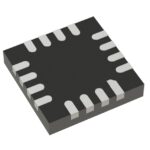 5PB1108CMGI8
The activity of extra discounts on wholesale prices is in full swing…
Please fill in your contact information and we will send you the latest wholesale price list.





