 ChipApex | Global Electronic Components Supplier
5SGSED6N2F45C2LN
Search Product
Search Post
— IC芯片 | 连接器 | 传感器 | 被动器件 —
Search productSearch post
— IC芯片 | 连接器 | 传感器 | 被动器件 —
Consult the customer manager about the wholesale price.
consultation hotline:86-132-6715-2157
email:[email protected]
Contact the product manager for consultation. One-stop consultation is available.
Do you want a lower wholesale price? Please send us your inquiry and we will reply immediately.
The Altera 5SGSED6N2F45C2LN is a Stratix V GS Field Programmable Gate Array (FPGA) designed for high-performance digital logic applications. It features 583,000 logic elements and 220,000 Adaptive Logic Modules (ALMs). The device includes 45 Mbit of embedded memory and supports 840 I/O pins. It operates within a junction temperature range of 0°C to 85°C and utilizes a 1932-ball FCBGA package. This component belongs to the Stratix V GS series, optimized for cost-effective scalability in communication and industrial sectors.
Verify component authenticity through authorized distributors or direct manufacturer channels due to potential availability constraints. Confirm RoHS compliance status and moisture sensitivity level (MSL 3) prior to handling. Ensure storage conditions meet J-STD-033 standards to prevent damage. Check for end-of-life notifications or obsolescence notices from Altera before finalizing procurement plans.
Select this model when requiring moderate logic density with low power consumption characteristics typical of the Stratix V GS family. Compare against the 5SGSED6N3F45C2G variant if extended temperature ranges or specific packaging options are required. Evaluate total memory requirements against the 45 Mbit limit to ensure sufficient on-chip resources for design implementation without excessive external memory dependencies.
This part is part of the broader Stratix V FPGA portfolio, which includes GX, GS, and SX variants. The GS series specifically targets cost-sensitive applications while maintaining high performance. It shares architectural similarities with other Stratix V devices but differs in logic density and transceiver configurations compared to higher-end models like the Stratix V GX.
Direct pin-to-pin replacements may not exist within the same family due to varying logic densities. Consider upgrading to Agilex series FPGAs for future-proofing, though this requires significant redesign. Verify compatibility with existing Quartus Prime software versions when evaluating alternative components.
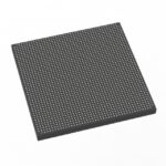 5SGSED6N2F45C2LN
The activity of extra discounts on wholesale prices is in full swing…
Please fill in your contact information and we will send you the latest wholesale price list.





