ChipApex | Global Electronic Components Supplier
5SGSMD5K2F40C3WN
Search Product
Search Post
— IC芯片 | 连接器 | 传感器 | 被动器件 —
Search productSearch post
— IC芯片 | 连接器 | 传感器 | 被动器件 —
Consult the customer manager about the wholesale price.
consultation hotline:86-132-6715-2157
email:[email protected]
Contact the product manager for consultation. One-stop consultation is available.
Do you want a lower wholesale price? Please send us your inquiry and we will reply immediately.
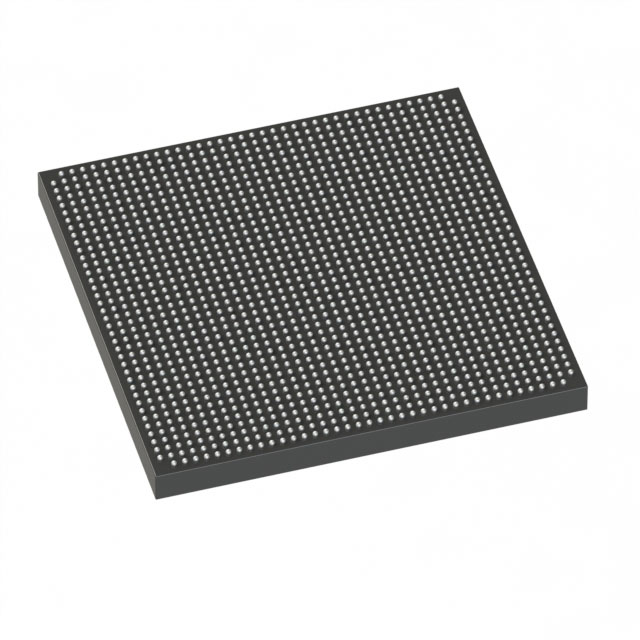
The Altera 5SGSMD5K2F40C3WN is a Stratix V GS Field Programmable Gate Array (FPGA) manufactured by Intel. It features 457,000 logic elements and 172,600 Adaptive Logic Modules (ALMs). The device includes 39 Mbits of embedded memory and supports 696 I/Os. It operates within a junction temperature range of 0°C to 85°C and utilizes a 1517-ball FCBGA package. This component is part of the Stratix V GS family, designed for bandwidth-centric applications.
Verify the specific suffix 'W' against official Intel documentation, as standard listings typically use 'C' or 'I' for commercial/industrial grades. Confirm availability status directly with authorized distributors, as lead times may vary significantly for this series. Ensure the package type matches the required PCB footprint.
Compare the 457,000 LE count and 39 Mbit memory capacity against project requirements. Verify that the 1517-ball FCBGA package fits the design constraints. Check if the 0°C to 85°C operating range meets environmental specifications. Consider power consumption relative to other Stratix V variants.
This FPGA belongs to the Stratix V GS family, which targets cost-sensitive, high-volume applications. It shares architectural similarities with the GX and GT families but focuses on reducing cost while maintaining essential performance metrics for general-purpose programmable logic needs.
Direct substitutes include other Stratix V GS devices with similar logic counts, such as the 5SGSMD5K2F40C3G or 5SGSMD5K2F40C1G. Verify pin compatibility and electrical characteristics before substitution.
 5SGSMD5K2F40C3WN
The activity of extra discounts on wholesale prices is in full swing…
Please fill in your contact information and we will send you the latest wholesale price list.