 ChipApex | Global Electronic Components Supplier
5SGSMD6N2F45I3N
Search Product
Search Post
— IC芯片 | 连接器 | 传感器 | 被动器件 —
Search productSearch post
— IC芯片 | 连接器 | 传感器 | 被动器件 —
Consult the customer manager about the wholesale price.
consultation hotline:86-132-6715-2157
email:[email protected]
Contact the product manager for consultation. One-stop consultation is available.
Do you want a lower wholesale price? Please send us your inquiry and we will reply immediately.
The Altera 5SGSMD6N2F45I3N is a Stratix V GS Field Programmable Gate Array featuring 840 I/Os and housed in a 1932-ball FCBGA package. It integrates 583,000 logic elements, 583,000 adaptive logic modules, and 46,080,000 total RAM bits. The device supports data rates up to 14.1 Gb/s with 48 transceivers. Operating voltage ranges from 0.82V to 0.88V, with an industrial temperature range of 0°C to 85°C.
Verify component authenticity through authorized channels due to potential supply chain variations. Confirm RoHS compliance status and moisture sensitivity level prior to assembly. Check for specific manufacturing date codes if long-term reliability is critical. Ensure ESD protection protocols are followed during handling. Validate pinout compatibility with existing PCB layouts before finalizing procurement decisions.
Select this model when balancing performance with cost efficiency in mid-to-high volume designs. Compare against Stratix V GX series if higher speed grades or extended temperature ranges are required. Evaluate power consumption profiles against available cooling solutions. Consider the 1932-ball package size for board space constraints. Verify Quartus Prime software version compatibility for design implementation.
This component belongs to the Altera Stratix V GS family, designed as a cost-optimized alternative to the GX series. It shares similar architectural features but targets applications where extreme performance is less critical than value. The GS series maintains robust I/O capabilities and significant logic density suitable for complex digital signal processing tasks.
Publicly confirmed direct substitutes are not identified in the provided documentation. Designers should consult official replacement guides for equivalent logic density and I/O counts within the Stratix V portfolio. Cross-referencing pinouts and electrical characteristics is essential when considering alternative FPGA families.


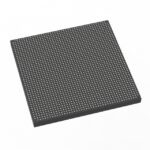 5SGSMD6N2F45I3N
The activity of extra discounts on wholesale prices is in full swing…
Please fill in your contact information and we will send you the latest wholesale price list.



