ChipApex | Global Electronic Components Supplier
5SGXEB5R3F43I3
Search Product
Search Post
— IC芯片 | 连接器 | 传感器 | 被动器件 —
Search productSearch post
— IC芯片 | 连接器 | 传感器 | 被动器件 —
Consult the customer manager about the wholesale price.
consultation hotline:86-132-6715-2157
email:[email protected]
Contact the product manager for consultation. One-stop consultation is available.
Do you want a lower wholesale price? Please send us your inquiry and we will reply immediately.
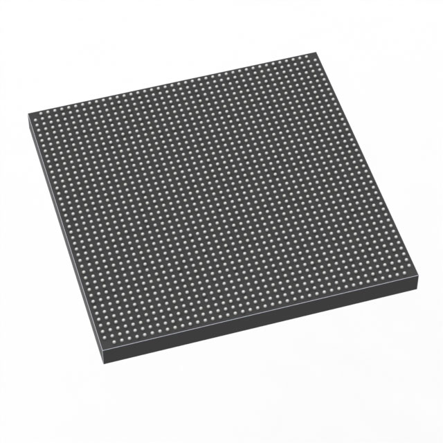
The Altera 5SGXEB5R3F43I3 is a Stratix V GX Field Programmable Gate Array (FPGA) designed for high-performance digital signal processing and networking applications. It features 2100 Logic Array Blocks (LABs), providing substantial logic density for complex designs. The device integrates 52 Mbits of embedded memory, including 6.88 Mbits of embedded block RAM (EBR), to support data buffering and storage needs. It includes 66 transceivers capable of operating at data rates up to 14.1 Gb/s, facilitating high-speed serial communications. The component offers 600 input/output pins and operates within a junction temperature range of -40°C to 100°C. It is housed in a 1760-pin FineLine Ball-Grid Array (FBGA) package.
Verify the exact ordering suffix and revision level against the manufacturer's current documentation, as legacy components may have multiple variants. Confirm RoHS compliance status and moisture sensitivity level (MSL) ratings prior to PCB assembly planning. Check for any active Process Change Notifications (PCNs) that might affect pinout or material composition. Ensure compatibility with the intended Quartus Prime software version for design implementation.
Select this model when the design requires the specific combination of 2100 LABs and 66 transceivers found in the Stratix V GX family. Compare against the 5SGXMB series if lower power consumption is critical, noting the distinct core voltage requirements. Evaluate the 1760-pin FBGA package constraints against available board space and thermal management capabilities. Ensure the application benefits from the 14.1 Gb/s transceiver speed rather than opting for lower-density alternatives.
This component belongs to the Stratix V GX family, which targets high-bandwidth applications such as telecom and datacom. It sits between the lower-density Stratix IV devices and the newer Agilex families in terms of architectural generation. The 'GX' designation specifically highlights its focus on high-speed serial transceiver performance compared to the GT or GS variants.
Publicly confirmed direct substitute part numbers are not available in the provided source material. Legacy FPGA replacements often require schematic and layout redesigns due to differences in pinouts, I/O standards, and internal architecture. Consult the manufacturer's migration guides for detailed compatibility information regarding newer device families.


 5SGXEB5R3F43I3
The activity of extra discounts on wholesale prices is in full swing…
Please fill in your contact information and we will send you the latest wholesale price list.