 ChipApex | Global Electronic Components Supplier
5SGXMA7H2F35C1WN
Search Product
Search Post
— IC芯片 | 连接器 | 传感器 | 被动器件 —
Search productSearch post
— IC芯片 | 连接器 | 传感器 | 被动器件 —
Consult the customer manager about the wholesale price.
consultation hotline:86-132-6715-2157
email:[email protected]
Contact the product manager for consultation. One-stop consultation is available.
Do you want a lower wholesale price? Please send us your inquiry and we will reply immediately.
The Altera 5SGXMA7H2F35C1WN is a high-performance Stratix V field-programmable gate array (FPGA) designed for demanding digital signal processing and communications applications. This device features a maximum of 690,000 logic elements and supports up to 1,488 DSP blocks with integrated multipliers. It includes extensive memory resources, comprising 10,080 Kbits of embedded memory and support for external memory interfaces. The component operates at a typical I/O voltage of 1.2V and utilizes a 20mm x 20mm FCBGA package with 1156 pins. It is rated for commercial temperature range operation from 0°C to 100°C.
Verify the specific suffix codes against official Intel/Altera documentation to confirm exact speed grade, package variant, and temperature rating. Ensure compatibility with existing board layouts regarding pin assignments and thermal requirements. Confirm that the supply chain source provides genuine components with traceability records to avoid counterfeit risks associated with legacy FPGA products.
Evaluate the design requirements against the available logic element count and DSP block availability to ensure sufficient capacity. Consider the pin count and I/O standards supported by the FCBGA package relative to system interconnect needs. Assess thermal dissipation requirements given the power consumption characteristics of the Stratix V family under full load conditions.
This component belongs to the Stratix V family, representing a generation of FPGAs focused on high throughput and low power efficiency. It succeeded earlier generations like Stratix IV, offering increased density and improved transceiver speeds. The part is intended for engineers requiring reconfigurable hardware acceleration in stationary or mobile base stations and enterprise networking gear.
Direct replacements may include other Stratix V variants with adjusted logic counts or package sizes. Cross-family migration to Agilex or Arria series requires significant architectural redesign due to differing interface and logic structures.
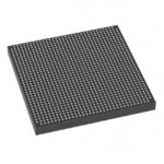 5SGXMA7H2F35C1WN
The activity of extra discounts on wholesale prices is in full swing…
Please fill in your contact information and we will send you the latest wholesale price list.





