 ChipApex | Global Electronic Components Supplier
SEARCH
Search Product
Search Post
— IC芯片 | 连接器 | 传感器 | 被动器件 —
Search productSearch post
— IC芯片 | 连接器 | 传感器 | 被动器件 —
Consult the customer manager about the wholesale price.
consultation hotline:86-132-6715-2157
email:[email protected]
Contact the product manager for consultation. One-stop consultation is available.
Do you want a lower wholesale price? Please send us your inquiry and we will reply immediately.
The 5T30553DCG8 is a low-power, high-performance clock buffer manufactured by Renesas Electronics. It features four outputs with low skew characteristics and supports input frequencies up to 200 MHz. The device operates within a supply voltage range of 1.71 V to 3.465 V and exhibits a maximum propagation delay of 4 ns. Designed for surface-mount applications, it is available in a tape-and-reel package configuration suitable for automated assembly processes.
Verify the specific suffix 'DCG8' corresponds to the required tape-and-reel packaging format. Confirm that the 1.71 V to 3.465 V supply voltage range aligns with the target system design. Ensure the -40°C to +105°C industrial temperature rating meets environmental requirements. Cross-reference the manufacturer part number with official Renesas documentation to confirm current production status.
Select this component when a single-input, four-output clock distribution solution is required. The 200 MHz maximum frequency capability suits moderate-to-high speed digital interfaces. The wide voltage tolerance allows flexibility in power domain integration. Verify that the 4 ns propagation delay fits the timing constraints of the destination logic elements.
This component belongs to the 5T30553 series of clock buffers. The 'DCG8' suffix indicates the specific package type and reel quantity configuration. It serves as a signal conditioning element within larger clock tree architectures, providing fan-out and isolation between source oscillators and multiple load points.
Consult official Renesas substitution guides for verified alternatives. Ensure any replacement maintains the 4-output topology and 200 MHz frequency limit. Verify pin compatibility if physical footprint retention is required.
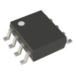 5T30553DCG8
The activity of extra discounts on wholesale prices is in full swing…
Please fill in your contact information and we will send you the latest wholesale price list.





