 ChipApex | Global Electronic Components Supplier
SEARCH
Search Product
Search Post
— IC芯片 | 连接器 | 传感器 | 被动器件 —
Search productSearch post
— IC芯片 | 连接器 | 传感器 | 被动器件 —
Consult the customer manager about the wholesale price.
consultation hotline:86-132-6715-2157
email:[email protected]
Contact the product manager for consultation. One-stop consultation is available.
Do you want a lower wholesale price? Please send us your inquiry and we will reply immediately.
The 5T93GL04PGGI8 is a high-performance, low-skew, low-jitter 1:4 LVCMOS clock buffer designed for PCI/PCI-X or networking applications. It features low input-to-output propagation delay and glitch-free output enable functionality. The device supports a 1.8V to 3.3V power supply range and operates within an industrial temperature range of -40°C to +85°C. Packaged in an 8-pin TSSOP format with a pitch of 0.65mm, it provides reliable clock distribution for high-speed digital systems requiring precise timing alignment.
Verify the specific package suffix PGGI8 corresponds to the 8-pin TSSOP variant with 0.65mm pitch. Confirm the operating temperature grade matches industrial requirements (-40°C to +85°C). Ensure compatibility with target system voltage levels (1.8V to 3.3V) before integration. Check for lead-free status if RoHS compliance is mandatory for the application.
Select this component when low jitter and skew are critical for PCI/PCI-X or networking interfaces. The 1:4 fan-out capability suits designs requiring single-source clock distribution to multiple synchronous loads. Consider the TSSOP package constraints for board space. Verify that the glitch-free enable feature meets the system's power-up sequencing requirements.
This part belongs to the 2304NZL family of LVCMOS clock buffers. It shares core architectural features such as low propagation delay and low output skew. The primary distinction lies in the specific package type and pin configuration associated with the PGGI8 suffix, which denotes the TSSOP form factor suitable for surface-mount assembly.
Direct substitutes include other members of the 2304NZL series, such as the 2304NZLDCGI or 2304NZLNTGI, provided the package type matches the design constraints. Verify electrical specifications and pinout compatibility before swapping packages.
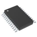 5T93GL04PGGI8
The activity of extra discounts on wholesale prices is in full swing…
Please fill in your contact information and we will send you the latest wholesale price list.






