 ChipApex | Global Electronic Components Supplier
SEARCH
Search Product
Search Post
— IC芯片 | 连接器 | 传感器 | 被动器件 —
Search productSearch post
— IC芯片 | 连接器 | 传感器 | 被动器件 —
Consult the customer manager about the wholesale price.
consultation hotline:86-132-6715-2157
email:[email protected]
Contact the product manager for consultation. One-stop consultation is available.
Do you want a lower wholesale price? Please send us your inquiry and we will reply immediately.
The Renesas 651SDCGI is a low-skew clock buffer from the 621S series, designed for high-speed signal distribution. It features four outputs and supports input frequencies up to 200 MHz. The device operates within a supply voltage range of 1.71 V to 3.465 V, accommodating 1.8 V to 3.3 V logic levels. Key electrical specifications include a maximum propagation delay of 4.5 ns and an RMS jitter performance of 50 fs. It is housed in a surface-mount tube package and functions reliably across an industrial temperature range of -40°C to +105°C.
Verify the specific suffix 'GI' against the official datasheet to confirm package type and tape/reel versus tube packaging options. Confirm RoHS compliance status directly from the manufacturer's documentation prior to ordering. Check current production lifecycle status to ensure long-term availability for design-in purposes.
Select this component when low phase noise and precise skew control are critical for system timing integrity. Ensure the required output load capacitance is within the specified limits for the 200 MHz operating frequency. Verify that the power supply voltage remains stable within the 1.71 V to 3.465 V window during all operational states.
This part belongs to the Renesas 621S series of clock buffers. It serves as a replacement for legacy low-skew drivers in high-performance computing and communication infrastructure designs where signal integrity is paramount. The 651SDCGI provides a compact solution for distributing reference clocks to multiple downstream components.
Consult the official Renesas cross-reference guide for verified pin-compatible alternatives. Ensure any substitute maintains the 50 fs RMS jitter specification and 200 MHz maximum input frequency capability.
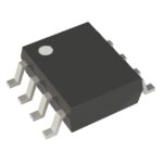 651SDCGI
The activity of extra discounts on wholesale prices is in full swing…
Please fill in your contact information and we will send you the latest wholesale price list.






