 ChipApex | Global Electronic Components Supplier
SEARCH
Search Product
Search Post
— IC芯片 | 连接器 | 传感器 | 被动器件 —
Search productSearch post
— IC芯片 | 连接器 | 传感器 | 被动器件 —
Consult the customer manager about the wholesale price.
consultation hotline:86-132-6715-2157
email:[email protected]
Contact the product manager for consultation. One-stop consultation is available.
Do you want a lower wholesale price? Please send us your inquiry and we will reply immediately.
The Texas Instruments 66AK2G12ABYA100 is a multicore System-on-Chip (SoC) based on the Keystone II architecture. It integrates one Arm Cortex-A15 subsystem and one C66x VLIW DSP core, both operating at up to 1 GHz. The device features extensive memory protection with ECC for L1/L2 data memory and shared SRAM. Key peripherals include two PRU-ICSS modules, a Gigabit Ethernet MAC with IEEE 1588v2 support, a crypto engine, and high-speed serial interfaces such as PCIe Gen 2 and dual USB 2.0 ports. It is housed in a 625-ball FCBGA package.
Verify the specific speed grade suffix '100' against the official datasheet to confirm the exact clock frequency configuration. Ensure that the ABY package type matches the target PCB footprint requirements. Confirm RoHS compliance status through the manufacturer's current documentation before finalizing procurement specifications.
Select this component when system design requires simultaneous real-time DSP processing and high-level OS management within a single chip. The integrated PRU-ICSS modules are suitable for deterministic control tasks requiring sub-microsecond latency. Consider the available GPIO count and peripheral interfaces to determine if external controllers are necessary for the application.
This part belongs to the 66AK2G1x family of heterogeneous multicore SoCs. These devices utilize the field-proven Keystone II architecture to enable flexible software designs centered on either the DSP or Arm cores. The family emphasizes reliability through extensive error correction code implementation across processor caches and shared memory structures.
Consult the official device comparison table for alternative parts within the 66AK2G1x series. Verify pin compatibility and feature parity if substituting with other variants in the same package.
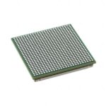 66AK2G12ABYA100
The activity of extra discounts on wholesale prices is in full swing…
Please fill in your contact information and we will send you the latest wholesale price list.






