 ChipApex | Global Electronic Components Supplier
SEARCH
Search Product
Search Post
— IC芯片 | 连接器 | 传感器 | 被动器件 —
Search productSearch post
— IC芯片 | 连接器 | 传感器 | 被动器件 —
Consult the customer manager about the wholesale price.
consultation hotline:86-132-6715-2157
email:[email protected]
Contact the product manager for consultation. One-stop consultation is available.
Do you want a lower wholesale price? Please send us your inquiry and we will reply immediately.
The SN74ALVC164245DLG4 is a 16-bit dual-supply bus transceiver designed for asynchronous communication between data buses. It features two independent power rails: Port A (VCCA) operates at 2.5 V or 3.3 V, while Port B (VCCB) supports 3.3 V or 5 V. This architecture enables level shifting between 2.5 V and 3.3 V environments, or between 3.3 V and 5 V systems. The device provides three-state outputs and is housed in a 48-pin SSOP package. It supports bidirectional data flow controlled by direction inputs.
Verify the specific suffix 'G4' to confirm lead-free and RoHS compliance status as per Texas Instruments documentation. Ensure the SSOP-48 package dimensions match the target PCB footprint requirements. Confirm that the operating temperature range of -40°C to +85°C aligns with the environmental conditions of the intended application design.
Select this component when interfacing logic families requiring translation between 2.5 V/3.3 V and 3.3 V/5 V supply voltages. The ALVC series offers lower power consumption compared to older LVC technologies. Ensure the system design accommodates the separate VCCA and VCCB power supplies to utilize the full level-shifting functionality effectively.
This part belongs to the SN74ALVC164245 family of widebus transceivers from Texas Instruments. It is functionally similar to the SN74ALVC164245 but distinguished by its specific 48-lead SSOP packaging variant. The device serves as a bridge for high-density data buses in mixed-voltage digital systems.
Direct pin-compatible substitutes include the SN74ALVC164245DGGT and SN74ALVC164245DGGR. Verify that alternative packages maintain identical electrical characteristics and pinout configurations before implementation.
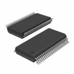 74ALVC164245DLG4
The activity of extra discounts on wholesale prices is in full swing…
Please fill in your contact information and we will send you the latest wholesale price list.






