 ChipApex | Global Electronic Components Supplier
SEARCH
Search Product
Search Post
— IC芯片 | 连接器 | 传感器 | 被动器件 —
Search productSearch post
— IC芯片 | 连接器 | 传感器 | 被动器件 —
Consult the customer manager about the wholesale price.
consultation hotline:86-132-6715-2157
email:[email protected]
Contact the product manager for consultation. One-stop consultation is available.
Do you want a lower wholesale price? Please send us your inquiry and we will reply immediately.
The Nexperia 74ALVCH16501DGGS is an 18-bit universal bus transceiver featuring 3-state outputs and bus hold inputs. It operates within a supply voltage range of 1.2 V to 3.6 V, supporting CMOS low power dissipation and direct interface with TTL levels. The device provides ±24 mA current drive at VCC = 3.0 V and includes IOFF circuitry for partial power-down applications. It complies with JEDEC standards JESD8-7, JESD8-5, and JESD8C/JESD36, offering ESD protection exceeding 2000 V (HBM) and 1000 V (CDM). The component is specified for operation from -40 °C to +85 °C and utilizes a TSSOP56 plastic thin shrink small outline package.
Verify the specific ordering suffix DGGS corresponds to the TSSOP56 package variant during procurement. Confirm that the required temperature range aligns with the -40 °C to +85 °C specification. Ensure design compatibility with the active HIGH OEAB and active LOW OEBA control signals. Check for any recent product change notices regarding the SOT364-1 package version.
Select this component when an 18-bit wide data path is required with flexible control over data flow direction. The inclusion of bus hold inputs simplifies PCB layout by reducing floating input risks. Verify that the operating voltage falls within the 1.2 V to 3.6 V range to ensure compliance with JEDEC standards. Consider the ±24 mA drive strength for load requirements.
This part belongs to the Nexperia ALVCH logic family, which is optimized for low-voltage, high-speed applications. The 74ALVCH16501 serves as a universal transceiver, distinct from simple buffers or drivers due to its latch/flip-flop capabilities. It is manufactured in a 56-lead TSSOP package, providing a compact solution for high-density digital systems.
Direct substitutes include the SN74ALVCH16501DGGR from Texas Instruments. Other compatible options may exist within the same ALVCH family from different manufacturers, provided pinouts and electrical characteristics match.
The IOFF circuitry disables the outputs when the device is powered down, preventing potentially damaging backflow current through the device.
A-to-B data flow is controlled by the output enable OEAB (active HIGH), latch enable LEAB, and clock CPAB inputs.
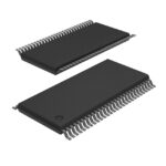 74ALVCH16501DGGS
The activity of extra discounts on wholesale prices is in full swing…
Please fill in your contact information and we will send you the latest wholesale price list.





