 ChipApex | Global Electronic Components Supplier
SEARCH
Search Product
Search Post
— IC芯片 | 连接器 | 传感器 | 被动器件 —
Search productSearch post
— IC芯片 | 连接器 | 传感器 | 被动器件 —
Consult the customer manager about the wholesale price.
consultation hotline:86-132-6715-2157
email:[email protected]
Contact the product manager for consultation. One-stop consultation is available.
Do you want a lower wholesale price? Please send us your inquiry and we will reply immediately.
The Nexperia 74AVC16836ADGG,118 is a 20-bit universal bus driver featuring registered outputs and Dynamic Controlled Output (DCO) circuitry. It operates within a supply voltage range of 1.2 V to 3.6 V and complies with JEDEC standards for low-voltage applications. The device utilizes a TSSOP56 package (SOT364-1) and supports an operating temperature range from -40 °C to +85 °C. Propagation delay varies by voltage: typical values are 2.4 ns at 1.65 V–1.95 V, 1.7 ns at 2.3 V–2.7 V, and 1.5 ns at 3.0 V–3.6 V.
Verify the specific ordering suffix
Select this component for designs requiring high-speed 20-bit data registration with noise reduction capabilities. Ensure the design accommodates the required number of VCC and GND pins for optimal performance. Verify that the application environment stays within the specified -40 °C to +85 °C temperature range and adheres to the recommended operating conditions for the chosen supply voltage.
This part belongs to the 74AVC16836A family of 20-bit registered drivers. It is distinct from similar parts like the 74ALVC16835ADGG,118, which is an 18-bit variant with different electrical characteristics. The 74AVC16836ADGG,118 specifically integrates DCO technology not found in standard bus transceivers.
Public confirmed substitute part numbers are not available in the provided documentation.
The DCO circuit initially lowers the output impedance to effectively drive the load during transitions and subsequently raises the impedance to reduce noise.
The LE input is active LOW. When LE is low, data on the clock (CP) edge is latched into the outputs. When LE is high, the outputs retain their previous state regardless of CP changes.
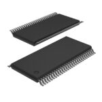 74AVC16836ADGG,118
The activity of extra discounts on wholesale prices is in full swing…
Please fill in your contact information and we will send you the latest wholesale price list.





