 ChipApex | Global Electronic Components Supplier
SEARCH
Search Product
Search Post
— IC芯片 | 连接器 | 传感器 | 被动器件 —
Search productSearch post
— IC芯片 | 连接器 | 传感器 | 被动器件 —
Consult the customer manager about the wholesale price.
consultation hotline:86-132-6715-2157
email:[email protected]
Contact the product manager for consultation. One-stop consultation is available.
Do you want a lower wholesale price? Please send us your inquiry and we will reply immediately.
The Nexperia 74AXP1T125GMH is a dual supply non-inverting buffer/line driver with 3-state output. It features one input (A), an output (Y), an output enable input (OE) and dual supply pins (VCCI and VCCO). The inputs are referenced to VCCI, which operates between 0.7 V and 2.75 V, while the output is referenced to VCCO, operating between 1.2 V and 5.5 V. This configuration enables voltage level translation. Schmitt-trigger action provides tolerance for slow input transitions. The device includes IOFF circuitry for partial power-down applications.
Verify the specific suffix 'MH' against official Nexperia documentation, as standard listings typically utilize 'GM', 'GN', 'GS', or 'GX'. Confirm package type SOT886 matches project requirements. Ensure design accounts for the specified temperature range of -40 °C to +85 °C. Validate that input and output supply voltages remain within the defined operational limits to prevent device damage.
Select this component when interfacing circuits with disparate supply voltages requiring robust signal integrity. The dual-supply design allows flexible voltage domain isolation. Consider the low input capacitance for high-frequency applications where signal loading must be minimized. Verify compatibility with system noise environments due to Schmitt-trigger input characteristics.
This device belongs to the 74AXP series, designed for advanced low-power applications. It utilizes Nexperia's proprietary technology to achieve high speed with minimal power dissipation. The XSON6 package offers a compact footprint suitable for space-constrained designs. It serves as a specialized solution for modern embedded systems requiring efficient voltage translation.
Standard equivalents include 74AXP1T125GM, 74AXP1T125GN, 74AXP1T125GS, and 74AXP1T125GX. These variants share identical electrical specifications but differ in package dimensions and thermal properties. Ensure pinout compatibility before substitution.
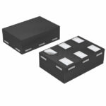 74AXP1T125GMH
The activity of extra discounts on wholesale prices is in full swing…
Please fill in your contact information and we will send you the latest wholesale price list.





