 ChipApex | Global Electronic Components Supplier
SEARCH
Search Product
Search Post
— IC芯片 | 连接器 | 传感器 | 被动器件 —
Search productSearch post
— IC芯片 | 连接器 | 传感器 | 被动器件 —
Consult the customer manager about the wholesale price.
consultation hotline:86-132-6715-2157
email:[email protected]
Contact the product manager for consultation. One-stop consultation is available.
Do you want a lower wholesale price? Please send us your inquiry and we will reply immediately.
The Nexperia 74AXP1T125GNH is a dual supply non-inverting buffer/line driver with 3-state output. It features one input (A), an output (Y), an output enable input (OE) and dual supply pins (VCCI and VCCO). The inputs are referenced to VCCI and the output is referenced to VCCO. All inputs can be connected directly to VCCI or GND. VCCI can be supplied at any voltage between 0.7 V and 2.75 V and VCCO can be supplied at any voltage between 1.2 V and 5.5 V.
Verify the specific package variant against the ordering information table. The 'GN' suffix corresponds to the XSON6 package (SOT1115) with dimensions 0.9 x 1.0 x 0.35 mm. Confirm temperature range is -40 °C to +85 °C. Ensure compatibility with required supply voltages: VCCI 0.7 V to 2.75 V and VCCO 1.2 V to 5.5 V. Check for RoHS compliance status if required by design specifications.
Select this component when interfacing circuits operating at different voltage levels, such as translating from low-voltage logic (e.g., 1.2 V) to higher voltage standards (e.g., 3.3 V or 5.5 V). The dual-supply architecture allows flexible power domain isolation. Consider the XSON6 package size for space-constrained designs. Verify that the input voltage does not exceed the maximum VCCI rating of 2.75 V under normal operation.
This device belongs to the 74AXP series of bus drivers designed for low-power applications. It is part of Nexperia's portfolio of logic ICs offering various package options including XSON and X2SON types. The 74AXP1T125 specifically addresses the need for level shifting in modern electronic systems where multiple voltage rails coexist.
Direct substitutes include other 74AXP1T125 variants with different packages such as 74AXP1T125GM (SOT886), 74AXP1T125GS (SOT1202), and 74AXP1T125GX (SOT1255-2). These share identical electrical characteristics but differ in physical footprint and thermal properties. Cross-referencing pinouts and package dimensions is essential for board-level replacement.
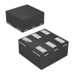 74AXP1T125GNH
The activity of extra discounts on wholesale prices is in full swing…
Please fill in your contact information and we will send you the latest wholesale price list.






