 ChipApex | Global Electronic Components Supplier
SEARCH
Search Product
Search Post
— IC芯片 | 连接器 | 传感器 | 被动器件 —
Search productSearch post
— IC芯片 | 连接器 | 传感器 | 被动器件 —
Consult the customer manager about the wholesale price.
consultation hotline:86-132-6715-2157
email:[email protected]
Contact the product manager for consultation. One-stop consultation is available.
Do you want a lower wholesale price? Please send us your inquiry and we will reply immediately.
The Renesas Electronics Corporation 74FCT3807QG8 is a single-input, ten-output clock buffer and driver belonging to the 74FCT series. It operates with an LVTTL input and provides CMOS/TTL outputs. The device supports a maximum frequency of 100 MHz and functions within a supply voltage range of 3V to 3.6V. Designed for surface-mount applications, it is housed in a 20-QSOP package (20-SSOP style, 0.154" width). The component is rated for commercial operating temperatures between 0°C and 70°C.
Verify the specific suffix 'G8' against the manufacturer's current datasheet to confirm package dimensions and lead finish specifications. Ensure the required operating temperature range aligns with the commercial grade (0°C to 70°C) rather than industrial variants. Confirm RoHS compliance status through official documentation prior to integration.
Select this component when a 1:10 clock split is required with LVTTL input compatibility. The 100 MHz frequency limit suits standard high-speed logic applications. Compare against the 74FCT3807AQG8 if extended industrial temperature ranges (-40°C to 85°C) are necessary, as both share similar electrical characteristics but differ in thermal ratings.
This part belongs to the broader 74FCT3807 family, which includes variants like the 74FCT3807QGI8 and 74FCT3807APYGI8. These siblings offer different performance metrics, such as higher frequencies up to 166 MHz or wider temperature ranges, while maintaining the same fundamental 1:10 buffering topology and pinout structure.
The 74FCT3807AQG8 serves as a parameter-equivalent alternative from Renesas, offering identical electrical functionality but with an extended industrial temperature range.
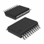 74FCT3807QG8
The activity of extra discounts on wholesale prices is in full swing…
Please fill in your contact information and we will send you the latest wholesale price list.





