 ChipApex | Global Electronic Components Supplier
SEARCH
Search Product
Search Post
— IC芯片 | 连接器 | 传感器 | 被动器件 —
Search productSearch post
— IC芯片 | 连接器 | 传感器 | 被动器件 —
Consult the customer manager about the wholesale price.
consultation hotline:86-132-6715-2157
email:[email protected]
Contact the product manager for consultation. One-stop consultation is available.
Do you want a lower wholesale price? Please send us your inquiry and we will reply immediately.
The Renesas Electronics Corporation 74FCT3807SOG is a single-input, ten-output clock buffer and driver designed for high-speed digital systems. Operating within a supply voltage range of 3 V to 3.6 V, this component supports a maximum output frequency of 166 MHz. It features CMOS and TTL compatible outputs and accepts LVTTTL inputs. The device is housed in a 20-pin SOIC package with surface mount installation. It operates reliably across a commercial temperature range from 0°C to +70°C, drawing a typical operating supply current of 15.5 mA.
Verify the specific suffix 'SOG' against the manufacturer's official datasheet to confirm pinout and electrical characteristics. Confirm RoHS compliance status through the latest environmental declaration. Check for any Product Change Notices (PCN) related to assembly facility changes or material substitutions before finalizing procurement orders.
Select the 74FCT3807SOG when a single source signal requires fan-out to ten destinations with CMOS or TTL interface compatibility. Ensure the application environment remains within the 0°C to +70°C operating temperature range. Verify that the system power supply stays strictly between 3 V and 3.6 V to maintain the specified 166 MHz performance limit.
This component belongs to the 74FCT3807 series of low-skew clock buffers. Related variants include the 74FCT3807APYGI8, which offers an extended industrial temperature range (-40°C to +85°C) in an SSOP package, and the 74FCT3807SQGI8, which provides low skew specifications in a reel packaging format. These variations share the core 1:10 distribution functionality but differ in thermal ratings and physical packaging.
Publicly documented substitutes include the IDT74FCT3807SOG. For alternative packages, the 74FCT3807APYGI8 serves as a functional equivalent with extended temperature capabilities. Always verify pin-to-pin compatibility and electrical parameter alignment with the original design requirements.
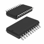 74FCT3807SOG
The activity of extra discounts on wholesale prices is in full swing…
Please fill in your contact information and we will send you the latest wholesale price list.






