 ChipApex | Global Electronic Components Supplier
SEARCH
Search Product
Search Post
— IC芯片 | 连接器 | 传感器 | 被动器件 —
Search productSearch post
— IC芯片 | 连接器 | 传感器 | 被动器件 —
Consult the customer manager about the wholesale price.
consultation hotline:86-132-6715-2157
email:[email protected]
Contact the product manager for consultation. One-stop consultation is available.
Do you want a lower wholesale price? Please send us your inquiry and we will reply immediately.
The SN74GTLPH1627 is an 18-bit bus transceiver providing LVTTL-to-GTLP and GTLP-to-LVTTL signal-level translation. It supports transparent and latched data transfer modes, with a clock-mode select (CMS) input for source-synchronous or clock-synchronous applications. The device features high-drive GTLP outputs of 100 mA and LVTTL outputs of ±24 mA. It includes Ioff, power-up 3-state, and BIAS VCC support for live insertion. The operating temperature range is -40°C to +85°C.
Verify the specific ordering suffix against the manufacturer's current documentation to confirm package type and tape-and-reel specifications. Confirm that the required termination voltage (VTT) and reference voltage (VREF) align with the GTLP or GTL standards supported by this component. Ensure design constraints regarding the 5-V tolerance on A-port inputs and control signals are met within the absolute maximum ratings.
Select this component when interfacing LVTTL logic with GTLP backplane architectures requiring high drive strength. Consider the flexible setup time adjustment (FSTA) feature if minimizing skew in source-synchronous designs is critical. Evaluate the need for adjustable edge-rate control (ERC) to optimize data-transfer rates and signal integrity based on the specific backplane load impedance.
This device belongs to the Widebus family from Texas Instruments. It incorporates TI-OPC circuitry to limit ringing on unevenly loaded backplanes and OEC circuitry to improve signal integrity while reducing electromagnetic interference. The part replaces functions of various 8-bit, 9-bit, 10-bit, and 16-bit transceivers and buffers, consolidating them into a single 18-bit solution.
SN74GTLPH1627DGGR
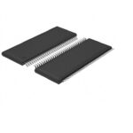 74GTLPH1627DGGRE4
The activity of extra discounts on wholesale prices is in full swing…
Please fill in your contact information and we will send you the latest wholesale price list.





