 ChipApex | Global Electronic Components Supplier

SEARCH
Search Product
Search Post
— IC芯片 | 连接器 | 传感器 | 被动器件 —
Search productSearch post
— IC芯片 | 连接器 | 传感器 | 被动器件 —
Consult the customer manager about the wholesale price.
consultation hotline:86-132-6715-2157
email:[email protected]
Contact the product manager for consultation. One-stop consultation is available.
Do you want a lower wholesale price? Please send us your inquiry and we will reply immediately.
The Nexperia 74HC1G32GW,165 is a single 2-input OR gate in the 74HC series. It operates on a supply voltage range of 2.0 V to 6.0 V with CMOS input levels. The device features clamp diodes for interfacing inputs exceeding VCC and provides symmetrical output impedance. It complies with JEDEC standards JESD8C and JESD7A. Static characteristics include an input leakage current of 1.0 µA maximum at 6.0 V and a supply current of 20 µA maximum. Dynamic performance specifies propagation delays up to 23 ns at 6.0 V with 50 pF load capacitance.
Verify the specific ordering suffix '165' against official Nexperia documentation, as standard commercial variants typically utilize suffixes such as '125'. Confirm package type SOT353-1 (TSSOP5) matches design requirements. Ensure compliance with RoHS and REACH regulations is documented for the specific batch. Check for automotive qualification status if intended for vehicle electronics.
Select this component when a single 2-input OR gate is required within the 74HC family specifications. It is suitable for designs needing operation across a wide voltage range from 2.0 V to 6.0 V. Consider the TSSOP5 package for space-constrained surface-mount applications. Verify that input signal levels align with CMOS thresholds rather than TTL levels, which are reserved for the HCT variant.
This part belongs to the Nexperia 74HC1G32 product line, which includes variants like 74HC1G32GW,125 and 74HC1G32GV,125. These devices share identical logical functionality but differ in packaging or manufacturing lot codes. The GW designation indicates the TSSOP5 plastic thin shrink small outline package. The product line is designed for general-purpose digital logic applications compliant with JEDEC standards.
Yes, the inputs include clamp diodes, enabling the use of current-limiting resistors to interface inputs to voltages in excess of VCC.
The device offers HBM protection exceeding 2000 V (Class 2) and CDM protection exceeding 1000 V (Class C3).
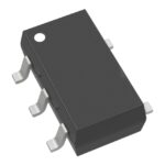 74HC1G32GW,165

The activity of extra discounts on wholesale prices is in full swing…
Please fill in your contact information and we will send you the latest wholesale price list.





