 ChipApex | Global Electronic Components Supplier

SEARCH
Search Product
Search Post
— IC芯片 | 连接器 | 传感器 | 被动器件 —
Search productSearch post
— IC芯片 | 连接器 | 传感器 | 被动器件 —
Consult the customer manager about the wholesale price.
consultation hotline:86-132-6715-2157
email:[email protected]
Contact the product manager for consultation. One-stop consultation is available.
Do you want a lower wholesale price? Please send us your inquiry and we will reply immediately.
The 74HCT14BQ,115 is a hex inverting Schmitt trigger manufactured by Nexperia USA Inc. It operates within a supply voltage range of 2.0 V to 6.0 V and complies with JEDEC standards JESD8C (2.7 V to 3.6 V) and JESD7A (2.0 V to 6.0 V). The device features TTL input levels, unlimited input rise and fall times, and ESD protection exceeding 2000 V (HBM) and 1000 V (CDM). It is specified for ambient temperatures from -40 °C to +125 °C and utilizes a DHVQFN14 package.
Verify the specific ordering suffix '115' corresponds to the DHVQFN14 package variant when sourcing. Confirm that the procurement channel provides the official Nexperia datasheet Rev. 10 dated 29 February 2024 to ensure accurate electrical parameter alignment. Cross-reference the manufacturer part number against authorized distributor databases to validate authenticity before finalizing acquisition.
Select this component for applications requiring signal conditioning with hysteresis to eliminate jitter on slowly changing inputs. The TTL input threshold compatibility allows direct interfacing with standard logic families without additional level shifting components. Ensure the design accommodates the thermal dissipation requirements associated with the DHVQFN14 package outline SOT762-1.
This device belongs to the 74HCT series of high-speed Si-gate CMOS logic devices. It is pin-compatible with Low-power Schottky TTL (LSTTL) standards. The product line includes variants such as the 74HC14 and 74HCT14, offering flexibility in input logic thresholds while maintaining identical physical footprints across different package options like SO14 and TSSOP14.
The 74HC14BQ,115 serves as a functional alternative but requires verification of input logic level compatibility, as it utilizes CMOS thresholds rather than TTL levels. Other package variants such as the 74HCT14D or 74HCT14PW may be considered if the DHVQFN14 footprint is not mandatory.
Schmitt trigger inputs transform slowly changing input signals into sharply defined, jitter-free output signals.
The input clamp diodes enable the use of current limiting resistors to interface inputs to voltages in excess of VCC.
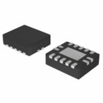 74HCT14BQ,115

The activity of extra discounts on wholesale prices is in full swing…
Please fill in your contact information and we will send you the latest wholesale price list.




