 ChipApex | Global Electronic Components Supplier

SEARCH
Search Product
Search Post
— IC芯片 | 连接器 | 传感器 | 被动器件 —
Search productSearch post
— IC芯片 | 连接器 | 传感器 | 被动器件 —
Consult the customer manager about the wholesale price.
consultation hotline:86-132-6715-2157
email:[email protected]
Contact the product manager for consultation. One-stop consultation is available.
Do you want a lower wholesale price? Please send us your inquiry and we will reply immediately.
74LVC1G00GW,165 is listed in the Inverter Gates range at ChipApex. The manufacturer field lists Nexperia USA Inc.. Its product description is IC GATE NAND 1CH 2-INP 5TSSOP. Review the specifications below when checking this part for your BOM.
The Nexperia 74LVC1G00GW,165 is a single 2-input NAND gate in a TSSOP5 (SOT353-1) package. It operates with a supply voltage range of 1.65 V to 5.5 V and features Schmitt-trigger inputs for noise immunity. The device includes IOFF circuitry for partial power-down mode operation, preventing backflow current. It supports direct interface with TTL levels and offers ±24 mA output drive at VCC = 3.0 V. Latch-up performance exceeds 250 mA per JESD 78 Class II. Operating temperature ranges from -40 °C to +125 °C.
Verify the specific ordering suffix
Select this component when a single 2-input NAND function is required in a compact surface-mount package. The TSSOP5 form factor suits space-constrained designs. Ensure the application voltage falls within the 1.65 V to 5.5 V range. Consider the Schmitt-trigger inputs if signal integrity is a concern due to slow transitions. Verify thermal dissipation requirements against the total power dissipation limits specified for the TSSOP5 package.
This part belongs to the 74LVC family of low-voltage CMOS logic gates. The 'GW' designation specifically identifies the TSSOP5 plastic thin shrink small outline package with a body width of 1.25 mm. The base type number is 74LVC1G00. This series is designed for wide supply voltage operation and compatibility with both 3.3 V and 5 V systems.
Direct pin-compatible replacements include other packages of the same logical function, such as 74LVC1G00GV (SC-74A), 74LVC1G00GM (XSON6), or 74LVC1G00GN (XSON6). Ensure the substitute matches the required package footprint and electrical specifications.
Yes, the device includes IOFF circuitry that disables the output when powered down, preventing potentially damaging backflow current through the device.
The inputs are overvoltage tolerant up to 5.5 V, even when the supply voltage (VCC) is lower, allowing safe interfacing with 5 V devices in 3.3 V systems.
Explore related parts through Logic, Integrated Circuits (ICs), all product categories, ChipApex homepage.
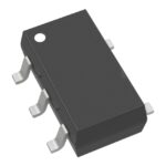 74LVC1G00GW,165

The activity of extra discounts on wholesale prices is in full swing…
Please fill in your contact information and we will send you the latest wholesale price list.




