 ChipApex | Global Electronic Components Supplier
SEARCH
Search Product
Search Post
— IC芯片 | 连接器 | 传感器 | 被动器件 —
Search productSearch post
— IC芯片 | 连接器 | 传感器 | 被动器件 —
Consult the customer manager about the wholesale price.
consultation hotline:86-132-6715-2157
email:[email protected]
Contact the product manager for consultation. One-stop consultation is available.
Do you want a lower wholesale price? Please send us your inquiry and we will reply immediately.
The 74LVC377DB,118 is an octal D-type flip-flop manufactured by Nexperia. It features positive-edge triggering and non-inverting outputs. The device operates within a supply voltage range of 1.2 V to 3.6 V. It is housed in a 20-SOIC package with a width of 7.50 mm. The component supports a maximum clock frequency of 230 MHz. Propagation delay is specified at 8.2 ns under standard load conditions. It includes a master reset function and maintains static current consumption of 10 µA. The operating temperature range extends from -40 °C to +125 °C.
Verify the specific suffix designation against official Nexperia documentation to confirm package type and tape/reel specifications. Confirm availability status as distribution channels may list obsolete or discontinued variants. Ensure compliance with RoHS and REACH regulations required for your manufacturing region. Cross-reference the manufacturer part number with authorized distributor catalogs to avoid counterfeit components. Validate that the selected variant matches the required thermal and electrical specifications for your target application environment.
Select this component when an octal storage element with high-speed performance is required. The 230 MHz clock capability suits high-frequency digital designs. The wide supply voltage range facilitates integration with various logic families. The SOIC package offers suitable PCB footprint constraints for surface-mount assembly. Consider the master reset feature if system initialization control is necessary. Evaluate the 24 mA output drive strength against load requirements.
This part belongs to the 74LVC series of low-voltage CMOS logic devices. The series is designed for applications requiring operation between 1.2 V and 3.6 V. The 74LVC377 specifically provides octal flip-flop functionality. It is part of Nexperia's extensive portfolio of standard logic integrated circuits. The device complements other LVC family members like latches and gates for complete digital system design.
The 74LVC377PW,118 serves as a pin-compatible alternative using a TSSOP package. Verify that the physical dimensions and lead pitch of the replacement package fit the existing PCB layout. Ensure electrical parameters such as propagation delay and output current remain within acceptable limits for the design.
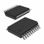 74LVC377DB,118
The activity of extra discounts on wholesale prices is in full swing…
Please fill in your contact information and we will send you the latest wholesale price list.






