 ChipApex | Global Electronic Components Supplier

SEARCH
Search Product
Search Post
— IC芯片 | 连接器 | 传感器 | 被动器件 —
Search productSearch post
— IC芯片 | 连接器 | 传感器 | 被动器件 —
Consult the customer manager about the wholesale price.
consultation hotline:86-132-6715-2157
email:[email protected]
Contact the product manager for consultation. One-stop consultation is available.
Do you want a lower wholesale price? Please send us your inquiry and we will reply immediately.
The Renesas Electronics Corporation 8535AG-01LF is a clock buffer and multiplexer IC housed in a 20-TSSOP package. It operates with a supply voltage range of 3.135V to 3.465V and supports a maximum frequency of 266 MHz. The device features a 2:4 input-to-output ratio, accepting LVCMOS or LVTTL inputs and providing LVPECL outputs. It functions within an ambient operating temperature range of -40°C to 85°C.
Verify the specific suffix '01' against official Renesas documentation to confirm pinout and electrical characteristics. Confirm RoHS compliance status for the specific manufacturing lot. Check current product lifecycle status as clock buffer availability may vary by region and date.
Select this component when a 2:4 conversion from single-ended logic levels (LVCMOS/LVTTL) to differential LVPECL is required. Ensure the design accommodates the 3.3V nominal supply voltage and the thermal requirements of the TSSOP-20 package within the specified industrial temperature range.
This part belongs to the 8535A family of high-performance clock solutions. It serves as a low-skew buffer designed to distribute clock signals in systems requiring precise timing. The device integrates multiplexing capabilities to select between input sources.
Publicly confirmed substitute part numbers are not available in the provided data. Verify compatibility with existing board layouts and signal integrity requirements before considering alternative components.
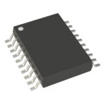 8535AG-01LF

The activity of extra discounts on wholesale prices is in full swing…
Please fill in your contact information and we will send you the latest wholesale price list.





