 ChipApex | Global Electronic Components Supplier

SEARCH
Search Product
Search Post
— IC芯片 | 连接器 | 传感器 | 被动器件 —
Search productSearch post
— IC芯片 | 连接器 | 传感器 | 被动器件 —
Consult the customer manager about the wholesale price.
consultation hotline:86-132-6715-2157
email:[email protected]
Contact the product manager for consultation. One-stop consultation is available.
Do you want a lower wholesale price? Please send us your inquiry and we will reply immediately.
The ICS859S1601I is a 16:1 LVCMOS/LVTTL-to-LVPECL/LVDS clock multiplexer from the HiPerClockS family. It accepts sixteen selectable single-ended clock inputs and provides one differential output pair configurable as LVPECL or LVDS via the SEL_OUT pin. The device operates up to 250MHz with a typical propagation delay of 1.0ns. It supports full 3.3V or 2.5V supply modes, features internal pull-downs on select pins, and includes an active-high output enable (OE) pin. Additive phase jitter is typically 0.20ps RMS at 155.52MHz.
Verify the specific ordering suffix against the manufacturer's current documentation. Suffixes such as 'LF' indicate lead-free/RoHS compliance, while 'T' denotes tape and reel packaging. Confirm that the required package type (Tube vs. Reel) matches the production needs. Ensure the voltage domain (3.3V or 2.5V) aligns with the system design before procurement.
Select this component when a 16:1 multiplexer interface between single-ended CMOS/TTL sources and differential LVPECL/LVDS loads is required. Choose based on the target supply voltage; note that LVDS operation requires floating VCC_TAP at 3.3V but connects it to VCC at 2.5V. Verify that the input clock frequencies do not exceed the 250MHz maximum rating and that the thermal environment supports the specified junction temperature limits.
The ICS859S1601I belongs to the IDT HiPerClockS family of high-performance clock solutions. It is manufactured by Integrated Device Technology (IDT), which was subsequently acquired by Renesas Electronics Corporation. The device is housed in a 28-lead TSSOP package with dimensions of 4.4mm x 9.7mm.
Publicly confirmed substitute part numbers are not available in the provided datasheet. Designers should consult the manufacturer for cross-reference information regarding newer generations or alternative multiplexers within the HiPerClockS portfolio.
The output level is controlled by the SEL_OUT pin. Driving SEL_OUT HIGH selects LVPECL levels, while driving it LOW selects LVDS levels.
VCC_TAP is a power supply pin. For LVPECL operation, it connects to VCC. For LVDS operation at 3.3V, it must be left floating; at 2.5V, it connects to VCC.
Unused CLK inputs can be left floating. For additional protection, a 1kΩ resistor may be tied from the input to ground, though this is not strictly required due to internal pulldowns.
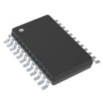 859S1601BGILF

The activity of extra discounts on wholesale prices is in full swing…
Please fill in your contact information and we will send you the latest wholesale price list.






