 ChipApex | Global Electronic Components Supplier

SEARCH
Search Product
Search Post
— IC芯片 | 连接器 | 传感器 | 被动器件 —
Search productSearch post
— IC芯片 | 连接器 | 传感器 | 被动器件 —
Consult the customer manager about the wholesale price.
consultation hotline:86-132-6715-2157
email:[email protected]
Contact the product manager for consultation. One-stop consultation is available.
Do you want a lower wholesale price? Please send us your inquiry and we will reply immediately.
The Renesas 87946AYI-147LF/W is a low skew, ÷1, ÷2 LVCMOS/LVTTL fanout buffer. It features ten single-ended outputs with 7Ω typical output impedance and two selectable single-ended clock inputs (CLK0/CLK1). The device supports frequencies up to 250 MHz. Supply voltage ranges are 2.375V–2.625V and 3.135V–3.465V. Operating temperature spans -40°C to +105°C. Package: 32-LQFP.
Verify the specific suffix 'W' against the manufacturer's datasheet to confirm RoHS compliance status and lead-free specifications. Ensure the package type matches the required 32-LQFP footprint. Confirm supply voltage requirements align with the specified dual range of 2.375V–2.625V and 3.135V–3.465V before procurement.
Select this component when a low skew fanout buffer with ten outputs is required. It supports both LVCMOS and LVTTL interfaces via selectable inputs. Verify that the operating temperature range of -40°C to +105°C meets system environmental constraints. Ensure the input frequency does not exceed 250 MHz for proper functionality.
This part belongs to the Renesas 87946 series of clock generators and support products. It functions as a fanout buffer designed to distribute clock signals with minimal skew. The series typically includes variants with different output counts and interface types, serving various digital system synchronization needs.
Consult official substitution lists for direct equivalents. Generic cross-references may lack verified electrical compatibility. Verify pinout and voltage levels before substituting.
The maximum operating frequency is 250 MHz.
The device provides ten single-ended LVCMOS/LVTTL outputs.
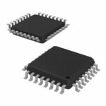 87946AYI-147LF/W

The activity of extra discounts on wholesale prices is in full swing…
Please fill in your contact information and we will send you the latest wholesale price list.






