 ChipApex | Global Electronic Components Supplier

SEARCH
Search Product
Search Post
— IC芯片 | 连接器 | 传感器 | 被动器件 —
Search productSearch post
— IC芯片 | 连接器 | 传感器 | 被动器件 —
Consult the customer manager about the wholesale price.
consultation hotline:86-132-6715-2157
email:[email protected]
Contact the product manager for consultation. One-stop consultation is available.
Do you want a lower wholesale price? Please send us your inquiry and we will reply immediately.
The 8L30205NLGI is a clock buffer integrated circuit manufactured by Renesas Electronics Corporation. It provides a 1:5 fanout ratio with a maximum operating frequency of 200 MHz. The device accepts multiple input types, including HCSL, LVCMOS, LVDS, LVPECL, LVTTL, and crystal oscillators. Outputs are configured as LVCMOS or LVTTL. It operates on a supply voltage ranging from 1.4V to 3.465V and functions within an ambient temperature range of -40°C to 85°C. The component is housed in a 24-VFQFN package with exposed pad.
Verify the specific suffix 'NLGI' against the manufacturer's datasheet to confirm pinout and electrical characteristics. Confirm RoHS3 compliance status and moisture sensitivity level (MSL 1) requirements during storage and handling. Ensure the 24-VFQFN thermal pad connection is properly managed for heat dissipation.
Select this component when a single-ended output buffer is required for differential or single-ended inputs up to 200 MHz. Verify that the load capacitance and drive strength requirements of the downstream logic align with the LVCMOS/LVTTL output specifications. Check supply voltage compatibility across the 1.4V to 3.465V range.
This part belongs to the 8L30205 family of low skew clock buffers. It serves as a signal integrity solution for distributing reference clocks in complex electronic designs. The VFQFN package offers a compact footprint suitable for space-constrained printed circuit board layouts.
Consult the official Renesas cross-reference documentation for verified substitutes. Generic equivalents may differ in input tolerance, output drive current, or phase jitter performance.
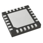 8L30205NLGI

The activity of extra discounts on wholesale prices is in full swing…
Please fill in your contact information and we will send you the latest wholesale price list.






