 ChipApex | Global Electronic Components Supplier

SEARCH
Search Product
Search Post
— IC芯片 | 连接器 | 传感器 | 被动器件 —
Search productSearch post
— IC芯片 | 连接器 | 传感器 | 被动器件 —
Consult the customer manager about the wholesale price.
consultation hotline:86-132-6715-2157
email:[email protected]
Contact the product manager for consultation. One-stop consultation is available.
Do you want a lower wholesale price? Please send us your inquiry and we will reply immediately.
8P34S2102NLGI is listed in the Clock Buffers, Drivers range at ChipApex. The manufacturer field lists Renesas Electronics Corporation. Its product description is IC CLK BUFFER 2:4 2GHZ 16VFQFPN. Review the specifications below when checking this part for your BOM.
The 8P34S2102NLGI is a high-performance, low-power differential dual 1:2 LVDS fanout buffer manufactured by Renesas Electronics. Designed for distributing high-frequency, very low additive phase-noise clock and data signals, it features two independent buffer channels with matched AC characteristics. The device supports fail-safe operation and accepts LVDS, LVPECL, and single-ended LVCMOS inputs on both differential CLKA/nCLKA and CLKB/nCLKB pins. It operates from a 1.8V or 2.5V supply voltage and is housed in a 16-lead VFQFPN package.
Verify the specific suffix 'NLGI' against the manufacturer's official datasheet to confirm pinout, packaging dimensions, and electrical tolerances. Ensure compatibility with the target PCB footprint for the 16-lead VFQFPN package. Confirm RoHS compliance status as per the latest product change notifications.
Select this component when dual-channel LVDS distribution with minimal skew is required. Verify that the input signal levels match the supported LVDS, LVPECL, or LVCMOS standards. Ensure the system power supply aligns with the 1.8V or 2.5V operating range specified for the device.
This part belongs to the 8P34S2102 series of clock buffers. It is characterized for operation within a temperature range of -40°C to +85°C. The device integrates bias voltage references to facilitate easy interfacing of AC-coupled signals to its inputs.
Both differential CLKA, nCLKA and CLKB, nCLKB inputs accept LVDS, LVPECL, and single-ended LVCMOS levels.
The output bank skew is typically 5ps.
Yes, the output amplitudes are selectable between 350mV and 500mV.
Explore related parts through Clock/Timing, Integrated Circuits (ICs), all product categories, ChipApex homepage.
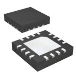 8P34S2102NLGI

The activity of extra discounts on wholesale prices is in full swing…
Please fill in your contact information and we will send you the latest wholesale price list.





